Page 34 - ChipScale_Mar-Apr_2020-digital
P. 34
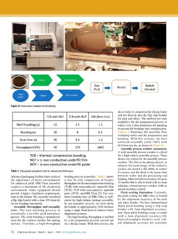
Figure 4: Process flow schematic for DBI bonding.
                                                                              diced wafer is cleaned on the dicing frame
                                                                              and fed directly into the flip-chip bonder
                                                                              for pick and place. The method not only
                                                                              simplifies the die preparation process to
                                                                              reduce cost, it also minimizes die handling
                                                                              to prevent die breakage and contamination.
                                                                              Figure 4 illustrates the assembly flow
                                                                              including wafer and die preparation and
                                                                              bonding. With this process, we have
                                                                              achieved assembly yield >90% with
                                                                              8x12mm size die, as shown in Figure 5.
                                                                                Assembly process window assessment.
                                                                              A wide assembly process window is critical
                                                                              for a high-volume assembly process. Three
                                                                              factors are critical for the assembly process
                                                                              window. The first is the plasma process to
                                                                              enhance the bond energy of the dielectric
                                                                              surface, the second is the ability to control
        Table 1: Throughput comparison table for various bond techniques.     Cu recess, and the third is the queue time
        Advanced packaging facilities have realized   bonding process is possible. Table 1 shows   between wafer and die processing and
        the importance of micro-environments   a side-by-side comparison of bonder   bonding. Material held in inventory for up to
        for enhanced yield. DBI Ultra assembly   throughput for thermocompression bonding   12 months that is able to bond with no issue
        requires a minimum of 1K cleanroom   (TCB) with nonconductive underfill film   indicates a broad process window with no
        environment. Some equipment should   (NCF), TCB with nonconductive underfill   special inventory control.
        provide a higher cleanliness requirement,   paste (NCP), and DBI Ultra [7]. The very   Pitch scaling limitation. Currently,
        such as the bonder. We currently retrofitted   short bonding time of DBI Ultra is well-  the pitch scaling for DBI Ultra is limited
        a flip-chip bonder with a class 100 clean kit   suited for high-volume package assembly.   by the alignment accuracy of the pick
        for our bonding experiment.        In our assembly process, we slow down   and place bonder. We have demonstrated
          Assembly throughput and assembly   the bonder to approximately 1600 die/hour   40µm pitch bonding using a flip-chip
        cost. The new bonding process is   using a single bond head to achieve better   bonder with 7µm alignment accuracy,
        essentially a no-flux pick-and-place   alignment accuracy.            and 10µm pitch bonding using a bonder
        process. The oxide bonding is spontaneous   The high bonding throughput is enabled   with a 1µm alignment accuracy [8].
        once the die surface touches the mating   by a die preparation process carried out   High-throughput bonders with sub-
        surface. Therefore, a high-throughput   on a dicing frame. With this process, the   µm alignment accuracy are currently

        32
        32   Chip Scale Review   March  •  April  •  2020   [ChipScaleReview.com]

