Page 30 - ChipScale_Mar-Apr_2020-digital
P. 30
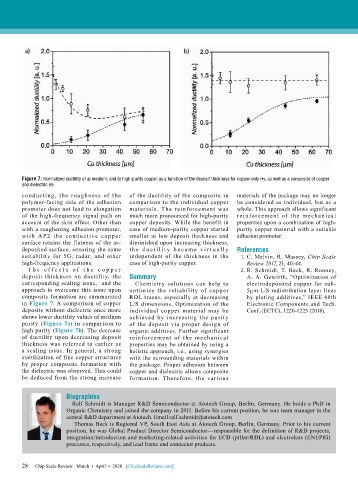
Figure 7: Normalized ductility of a) medium; and b) high-purity copper as a function of the deposit thickness for copper only (•), as well as a composite of copper
        and dielectric (•).
        conducting, the roughness of the   of the ductility of the composite in   materials of the package may no longer
        polymer-facing side of the adhesion   comparison to the individual copper   be considered as individual, but as a
        promoter does not lead to elongation   materials. The reinforcement  was   whole. This approach allows significant
        of the high-frequency signal path on   much more pronounced for high-purity   reinforcement of the mechanical
        account of the skin effect. Other than   copper deposits. While the benefit in   properties upon a combination of high-
        with a roughening adhesion promoter,   case of medium-purity copper started   purity copper material with a suitable
        with A P2 the conductive copper    smaller at low deposit thickness and   adhesion promoter.
        surface retains the flatness of the as-  diminished upon increasing thickness,
        deposited surface, ensuring the same   t h e d u c t i l i t y b e c a m e v i r t u a l l y   References
        suitability for 5G, radar, and other    independent of the thickness in the   1. C. Melvin, R. Massey, Chip Scale
        high-frequency applications.       case of high-purity copper.            Review 2017, 21, 40-44.
          T h e  e f f e c t s o f  t h e  c o p p e r                          2. R. Schmidt, T. Beck, R. Rooney,
        deposit thickness on ductility, the   Summary                             A. A. Gewirth, “Optimization of
        corresponding scaling issue,  and the   Chemistry solutions can help to   electrodeposited copper for sub-
        approach to overcome this issue upon   optimize the reliability of copper   5µm L/S redistribution layer lines
        composite formation are summarized   RDL traces, especially at decreasing   by plating additives,” IEEE 68th
        in Figure 7. A comparison of copper   L/S dimensions. Optimization of the   Electronic Components and Tech.
        deposits without dielectric once more   individual copper material may be   Conf. (ECTC), 1220-1225 (2018).
        shows lower ductility values of medium   achieved by increasing the purity
        purity (Figure 7a) in comparison to   of the deposit  via proper design of
        high purity (Figure 7b). The decrease   organic additives. Further significant
        of ductility upon decreasing deposit   reinforcement of the mechanical
        thickness was referred to earlier as   properties may be obtained by using a
        a scaling issue. In general, a strong   holistic approach, i.e., using synergies
        stabilization of fine copper structures   with the surrounding materials within
        by proper composite formation with   the package. Proper adhesion between
        the dielectric was observed. This could   copper and dielectric allows composite
        be deduced from the strong increase   formation. Therefore, the various


                       Biographies
                         Ralf Schmidt is Manager R&D Semiconductor at Atotech Group, Berlin, Germany. He holds a PhD in
                       Organic Chemistry and joined the company in 2011. Before his current position, he was team manager in the
                       central R&D department at Atotech. Email ralf.schmidt@atotech.com
                          Thomas Beck is Regional VP, South East Asia at Atotech Group, Berlin, Germany. Prior to his current
                       position, he was Global Product Director Semiconductor—responsible for the definition of R&D projects,
                       integration/introduction and marketing-related activities for ECD (pillar/RDL) and electroless (ENEPIG)
                       processes, respectively, and lead frame and connector products.


        28   Chip Scale Review   March  •  April  •  2020   [ChipScaleReview.com]
        28

