Page 26 - ChipScale_Mar-Apr_2020-digital
P. 26
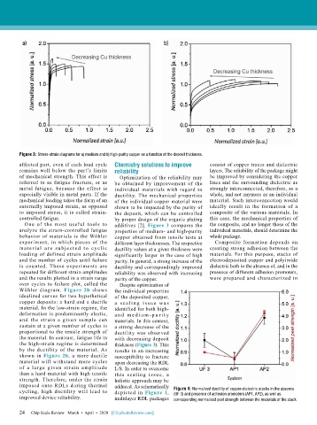
Figure 3: Stress-strain diagrams for a) medium and b) high-purity copper as a function of the deposit thickness.
        affected part, even if each load cycle   Chemistry solutions to improve   consist of copper traces and dielectric
        remains well below the part’s limits   reliability                    layers. The reliability of the package might
        of mechanical strength. This effect is   Optimization of the reliability may   be improved by considering the copper
        referred to as fatigue fracture, or as   be obtained by improvement of  the   lines and the surrounding dielectric as
        metal fatigue, because the effect is   individual materials with regard to   strongly interconnected, therefore, as a
        especially visible in metal parts. If the   ductility. The mechanical properties   whole, and not anymore as an individual
        mechanical loading takes the form of an   of the individual copper material were   material. Such interconnection would
        externally imposed strain, as opposed   shown to be impacted by the purity of   ideally result in the formation of a
        to imposed stress, it is called strain-  the deposit, which can be controlled   composite of the various materials. In
        controlled fatigue.                by proper design of the organic plating   this case, the mechanical properties of
          One of the most useful tools to   additives [2]. Figure 3 compares the   the composite, and no longer those of the
        analyze the strain-controlled fatigue   properties of medium- and high-purity   individual materials, should determine the
        behavior of materials is the Wöhler   copper obtained from tensile tests at   whole package.
        experiment, in which pieces of the   different layer thicknesses. The respective   Composite formation depends on
        mater ial a re subjected to cyclic   ductility values at a given thickness were   creating strong adhesion between the
        loading of defined strain amplitude   significantly larger in the case of high   materials. For this purpose, stacks of
        and the number of cycles until failure   purity. In general, a strong increase of the   electrodeposited copper and polyimide
        is counted. These experiments are   ductility and correspondingly improved   dielectric both in the absence of, and in the
        repeated for different strain amplitudes   reliability was observed with increasing   presence of different adhesion promoters,
        and the results plotted in a strain range   purity of the copper.     were prepared and characterized in
        over cycles to failure plot, called the   Despite optimization of
        Wöhler diagram.  Figure 2b shows   the individual properties
        idealized curves for two hypothetical   of the deposited copper,
        copper deposits: a hard and a ductile   a s c a l i ng i s s ue wa s
        material. In the low-strain regime, the   identified for both high-
        deformation is predominantly elastic,   a n d  m e d i u m - p u r i t y
        and the strain a given sample can   materials. In this context,
        sustain at a given number of cycles is   a strong decrease of the
        proportional to the tensile strength of   ductility was observed
        the material. In contrast, fatigue life in   with decreasing deposit
        the high-strain regime is determined   thickness (Figure 3). This
        by the ductility of the material. As   results in an increasing
        shown in Figure 2b, a more ductile   susceptibility to fracture
        material will withstand more cycles   upon decreasing the RDL
        of a  large given  strain amplitude   L/S. In order to overcome
        than a hard material with high tensile   this scaling issue, a
        strength. Therefore, under the strain   holistic approach may be
        imposed onto RDLs during thermal   adduced. As schematically
        cycling, high ductility will lead to   depicted in  Figure 1,   Figure 4: Normalized ductility of copper-dielectric stacks in the absence
                                                                 (UF 3) and presence of adhesion promoters (AP1, AP2), as well as
        improved device reliability.       multilayer RDL packages  corresponding normalized peel strength between the materials of the stack.

        24   Chip Scale Review   March  •  April  •  2020   [ChipScaleReview.com]
        24

