Page 28 - ChipScale_Mar-Apr_2020-digital
P. 28
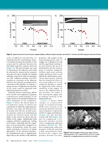
Figure 5: Copper thickness in the area of fracture for deposits obtained a) without an adhesion promoter, and b) with AP2. The insets show SEM micrographs of the area of fracture.
        terms of adhesion and ductility. As   promoter. The copper in the
        expected from the considerations above,   long delamination zone of
        a correlation between the ductility of the   sample (a) is thinned out and
        system and the adhesion between the   exhibits significant necking in
        individual materials could be observed   an area between the onset of
        (Figure 4). The peel strength was used   delamination and the fracture
        to characterize the adhesion and could   point. In contrast, sample (b)
        be obtained by measuring the required   exhibits much more uniform
        force per unit area to separate two bonded   copper thickness close to and
        materials, whereat the angle of separation   behind the delamination point.
        was 180°. Adhesion promoter one (AP1)   These observations indicate
        resulted in a decrease of the adhesion   that the beneficial effect of
        between the materials accompanied by   increased adhesion on the
        a decrease of the ductility. In contrast, a   composite ductility is caused
        strong increase of adhesion and ductility   by suppression of the necking
        of  the stack  could be obtained with   instability in the copper. As
        adhesion promoter two (AP2).       soon as the adhesion fails at
          Scanning electron microscopy (SEM)   any location, this effect is
        cross sections were employed to generate   lost, leaving the copper free
        a mechanistic understanding of the   to undergo necking in the
        improvement of the mechanical properties   delaminated zone.
        upon formation of the composite.     F i g u r e  6  s ho w s S E M
        Figure 5 shows the failure mode of   i m a g e s a t c o m p a r a b l e
        Cu-dielectric stacks in tensile test   scales of focused ion beam
        experiments in which the copper-polymer   (FIB) cross sections of the
        interface was either left untreated (a),   untreated interface between
        or treated with AP2 (b). In both cases,   electrochemical  deposition
        the interface underwent delamination   (ECD) of copper and dielectric
        around  the  fracture  point  and  the   (Figure 6a), the interface
        shape of the metal tip shows ductile   treated with AP2 (Figure 6b),
        failure of the copper. Additionally, both   and for comparison, a Cu-
        samples exhibited significant curling   dielectric interface treated
        after failure, indicating that the copper   with a roughening adhesion
        layer was permanently elongated by   promoter  (Figure 6c).  The
        plastic deformation, while the more   non-roughening ad hesion
        elastic polyimide reverted to its initial   promoter works by inserting
        dimensions. At the untreated interface,   a thin, nonconductive layer
        the delamination zone is significantly   b e t we e n t h e c o p p e r a n d   Figure 6: SEM micrographs of high-purity copper a) without
        larger than at the interface with adhesion   polymer. Because it is non-  adhesion promoter, and b) treated with AP2, as well as c) copper
                                                                      treated with a roughening adhesion promoter for comparison.

        26   Chip Scale Review   March  •  April  •  2020   [ChipScaleReview.com]
        26

