Page 32 - ChipScale_Mar-Apr_2020-digital
P. 32
stage of bonding (Figure 3a) includes
                                                                              the ultra-smooth oxide surfaces that bond
                                                                              spontaneously on contact, forming a
                                                                              protective seal around the metal pads at
                                                                              ambient. The metal pads are purposely
                                                                              recessed from the oxide surface to avoid
                                                                              interference with the oxide bonding. The
                                                                              bonded structures then go through a heated
                                                                              batch anneal. During the anneal, the metal
                                                                              pads expand to close the narrow gap between
                                                                              the top and bottom pads and metal diffuses
                                                                              across the interface to form permanent all-
                                                                              Cu bonding (Figure 3b). High assembly
                                                                              yield requires a surface topography of
                                                                              smooth oxide for the spontaneous dielectric-
                                                                              to-dielectric bonding and a uniform bond
                                                                              pad recess across the entire wafer. A pristine
                                                                              surface during bonding is critical to ensure a
                                                                              void-free bond interface. Finally, in order for
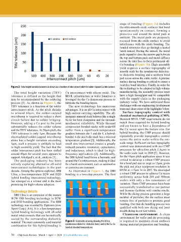
        Figure 2: Total height variation tolerance is shown as a function of interconnect pitch for solder-capped Cu interconnect.  the technology to be adopted in high-volume
          The total height variation (THV)   Cu interconnect with silicon oxide. The   manufacturing, the assembly process must
        tolerance is defined as the height that   BEOL infrastructure in wafer foundries is   have a high throughput and be compatible
        may be accommodated by the soldering   leveraged for the Cu damascene process to   with the supply chain in the packaging
        process [3]. As shown in Figure 2, the   fabricate the bonding layers.  industry today. We have addressed these
        THV tolerance is a function of the solder   The new technology has numerous   challenges with our engineering development
        interconnect pitch. As the pitch shrinks   advantages. It is an all-Cu interconnect with   team and share some of the highlights below.
        to  around  60μm,  the  solder-capped   high current carrying capability. The all-  Surface topography control with
        microbump is required to reduce a short   inorganic material stack behaves like a single   chemical mechanical polishing (CMP).
        circuit failure due to solder bridging.   Si die for heat dissipation and for thermal-  Standard BEOL CMP requirements do not
        However, adding a Cu post to the joint   mechanical reliability. While thermal   match those required for hybrid bonding
        substantially reduces the solder volume   compression bonded stacks with underfill   and are known to have a dependence of
        and the THV tolerance. At 20µm pitch, the   suffer from a significant temperature   the Cu recess upon the feature size. For
        THV tolerance is only 1µm. Because the   gradient between die 1 and die 4, a hybrid-  hybrid bonding, the CMP process should
        electroplated solder-capped microbump   bonded 4-die and 8-die stack has a minimal   repeatedly provide topographic control
        alone has a height variation exceeding   temperature gradient [2]. Additionally, the   across the entire wafer within the nm-
        1µm, such a process is unlikely to lead   small size interconnect creates a greatly   scale range. Sufficient surface topography
        to high assembly yield. The fact that the   reduced parasitic resistance, capacitance,   control was demonstrated with our CMP
        solder interconnect pitch has been stalled   and inductance, which is ideal for high-  processes for ultra-fine pitch (1.6µm) in
        around 40µm for several years appears to   frequency applications [2]. Additionally,   the wafer scale back in 2009 [5]. However,
        support Arkalgud’s, et al., analysis [3].  the DBI hybrid bond forms a hermetic seal   for the 40µm pitch application space it was
          The packaging industry has been   around the Cu interconnects, making it ideal   critical to develop a robust CMP process
        actively exploring alternative all-solid   for a harsh environment, such as automotive   for a bond pad size as large as 15µm, given
        interconnect technologies in the past   or corrosive environment.     the pick and place equipment resolution in
        decade. Among the options explored, DBI   As illustrated in Figure 3, the DBI   HVM at +/-7µm 3σ in 2017. We developed
        Ultra, a low-temperature D2W and D2D   bonding is a two-step process. The first   a robust CMP process to achieve Cu recess
        hybrid bonding interconnect technology,                               uniformity across both 200 and 300mm
        has emerged as a winner and is the most                               wafers with only a few nanometers of
        promising for high-volume adoption.                                   variation. These CMP processes have been
                                                                              successfully transferred to our partner
        Technology details                                                    and licensee facilities with similar results.
          DBI Ultra is an extension of the mature                             While the dicing process generates a large
        W2W DBI bonding technology to D2W                                     number of particles; the die surface must
        and D2D bonding applications. The DBI                                 remain free of particles to promote good
        technology was invented by Ziptronix (now                             bonding. Our thin die handling process was
        Xperi Corp.) [4-6]. It is a low-temperature                           qualified with both saw dicing and laser
        hybrid bonding technology with all-solid                              stealth dicing in our test vehicle.
        metal interconnects that are hermetically                               Cleanroom environment. A clean
        sealed by the surrounding dielectric                                  environment for wafer and die processing
        material. The most commonly used material   Figure 3: Schematic drawing showing the DBI a)   is required to maintain clean surfaces
        combination for this hybrid bonding is   spontaneous dielectric-dielectric bond; and b) the Cu-Cu   during material preparation and bonding.
                                           bond at elevated temperatures.

        30
        30   Chip Scale Review   March  •  April  •  2020   [ChipScaleReview.com]

