Page 31 - ChipScale_Mar-Apr_2020-digital
P. 31
Die-to-wafer hybrid bonding for 2.5D and


        3D integration


        By Laura Mirkarimi, Guilian Gao  [Xperi Corporation]
        A         s Moore’s law is reaching   The die-to-wafer (D2W) hybrid bonding   Challenges with solder


                  a physical limit, continued
                  market pressure drives the   technology we describe promises to   interconnect/fine pitch
                                           revolutionize the packaging industry.
                                                                                Significant height variations can
        interconnect density higher, requiring   Currently, two application areas are the   be realized across wafers prepared in
        finer pitch wafer package technology with   focus of the industry. The first application   standard processing, because each step
        stacking solutions. While solder flip-chip   area is in 3D stacking of high-bandwidth   of making the die and substrate ready for
        technology has enabled continuous die and   memory (HBM)/dynamic random access   bonding introduces thickness variations.
        package pitch scaling over the past five   memory (DRAM) to replace the thermal   For example, the plated bump height
        decades, it appears to have reached its limits   compression solder-capped microbump   uniformity across a wafer can vary by 5
        around 40µm for volume manufacturing.   in the sub-40µm pitch range. The second   to 10% because of electroplating process
        Shrinking solder volumes much below a   application targets an ultra-high density   nonuniformity. In addition to the local
        40µm pitch creates a yield loss at assembly   interconnect at a 1µm pitch for compute-   solder height variation, the die may have
        from solder bridging or opens, and at   intensive chipsets. Interconnect scaling   an overall warp from the unbalanced build-
        environmental stress tests due to fatigue   to sub-micron pitch between die will   up differences on each side of the die (i.e.,
        failures from embrittlement of the solder.   enable widespread disaggregation for   solder ball on one side and not the other).
        The industry consensus has settled on the   high-bandwidth applications in the   A flip-chip solder ball connects the top
        need for a new, all-solid and preferably   future. In the near term, the transition   and bottom pads of an interconnect pair
        all-Cu interconnect technology. An all-  from solder to all Cu for current 3D and   during solder melting and solidification.
        Cu interconnect is particularly attractive   2.5D stacking applications offers a more   Because the liquid solder can be deformed
        for its high current carrying capability   reliable interconnect formed at 200ºC, with   easily in the molten stage and retain the
        and resistance to reliability failures. With   exceptional electrical performance because   deformed shape upon solidification, the
        a single component interconnect, there   of the smaller parasitics associated with   soldering process compensates for some
        is no driving force for inter-diffusion,   each Cu interconnect [2].  degree of height variation. When the
        unlike solder-based interconnect structures   We review the DBI Ultra technology   height difference of the opposing joints are
        like solder-capped/Cu/under bump   with a 40µm pitch test vehicle and compare   beyond the solder deformation limits, over
        metallization (UBM). However, historically   it with the current solder microbump   compression can cause the neighboring
        an all-Cu interconnect was believed to   technology. As with any new technology,   solder balls to bridge and form a short
        require thermal budgets of 400ºC to join   the barriers to adoption are lowered when   circuit failure, while excessive stretching
        the Cu pads, which would exclude a large   it is compatible with the industry supply   can cause the solder ball to break and
        number of products that require maximum   chain. We discuss the compatibility of this   induce an open circuit failure. Some of the
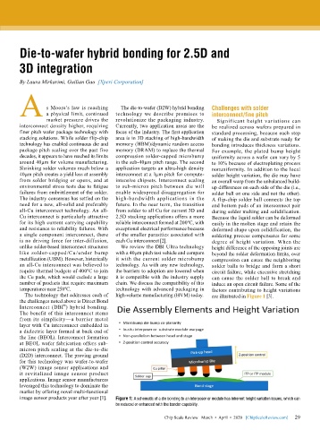
        temperatures near 250ºC.           technology with advanced packaging in   factors contributing to height variations
          The technology that addresses each of   high-volume manufacturing (HVM) today.   are illustrated in Figure 1 [3].
        the challenges noted above is Direct Bond
                        ®
        Interconnect (DBI ) hybrid bonding.
        The benefit of this interconnect stems
        from its simplicity—a barrier metal
        layer with Cu interconnect embedded in
        a dielectric layer formed at back end of
        the line (BEOL). Interconnect formation
        at BEOL wafer fabrication offers sub-
        micron pitch scaling at the die-to-die
        (D2D) interconnect. The proving ground
        for this technology was wafer-to-wafer
        (W2W) image sensor applications and
        it revitalized image sensor product
        applications. Image sensor manufacturers
        leveraged this technology to dominate the
        market by offering novel multi-functional
        image sensor products year after year [1].  Figure 1: A schematic of a die bonding to an interposer or module has inherent height variation issues, which can
                                           be reduced or enhanced with the bonder capability.

                                                                                                             29
                                                             Chip Scale Review   March  •  April  •  2020   [ChipScaleReview.com]  29

