Page 25 - ChipScale_Mar-Apr_2020-digital
P. 25
Holistic approach to improve the reliability of


        sub-5µm L/S Cu RDLs


        By Ralf Schmidt, Jan Knaup, Ulrich Memmert, Jens Palm, Cornelia Jäger, Stefan Pieper, Uwe Kirbach, Thomas Beck  [Atotech Group]
        A         d va n c e d  p a c k a g i ng


                  t e c h n o l og ie s  e n a b l e
                  f a s t er ,  t h i n n er ,  a n d
        m o r e  ef f ic ie n t  m o bi le  d e v ic e s .
        In  particular, fan-out wafer-level
        packaging (FOWLP) allows for higher
        performance, decreasing form factor,
        and significant cost reduction [1].
        Redistribution layers (RDLs) serve as
        rerouting of the connections within
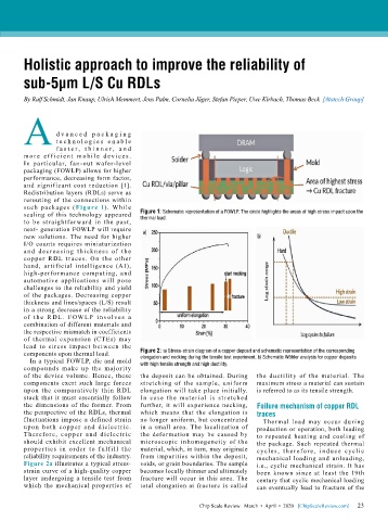
        such packages (Figure 1). While
        scaling of this technology appeared   Figure 1: Schematic representation of a FOWLP. The circle highlights the areas of high stress impact upon the
        to be straightforward in the past,   thermal load.
        next- generation FOWLP will require
        new  solutions.  The  need  for  higher
        I/O counts requires miniaturization
        a nd decreasi ng t h ick ness of t he
        copper R DL traces. On the other
        hand,  artificial  intelligence  (AI),
        high-performance computing, and
        automotive applications will pose
        challenges to the reliability and yield
        of the packages. Decreasing copper
        thickness and lines/spaces (L/S) result
        in a strong decrease of the reliability
        of t he R DL . FOW LP i nvolve s a
        combination of different materials and
        the respective mismatch in coefficients
        of thermal expansion (CTEs) may
        lead to stress impact  between  the
        components upon thermal load.      Figure 2: a) Stress-strain diagram of a copper deposit and schematic representation of the corresponding
          In a typical FOWLP, die and mold   elongation and necking during the tensile test experiment. b) Schematic Wöhler analysis for copper deposits
                                           with high tensile strength and high ductility.
        compounds make up the majority
        of the device volume. Hence, these   the deposit can be obtained. During   the  ductility  of  the  material.  The
        components exert such large forces   stretching of the sample, uniform   maximum stress a material can sustain
        upon  the  comparatively  thin  RDL   elongation will take place initially.   is referred to as its tensile strength.
        stack that it must essentially follow   In case the material is st retched
        the dimensions  of the former. From   further,  it  will  experience  necking,   Failure mechanism of copper RDL
        the perspective of the RDLs, thermal   which  means that the  elongation is   traces
        fluctuations impose a defined strain   no longer uniform, but concentrated   Thermal load may occur during
        upon both copper and dielectric.   in a  small  area. The  localization  of   production or operation, both leading
        Therefore,  copper  and  dielect r ic   the deformation may be caused by   to repeated heating and cooling of
        should exhibit excellent mechanical   microscopic inhomogeneity of the   the package. Such repeated thermal
        proper ties in order to f ulf ill the   material, which, in turn, may originate   cycle s, t he refore, i nduce cycl ic
        reliability requirements of the industry.   from impurities within the deposit,   mechanical loading and unloading,
        Figure 2a illustrates a typical stress-  voids, or grain boundaries. The sample   i.e., cyclic mechanical strain. It has
        strain curve of a high-quality copper   becomes locally thinner and ultimately   been known since at least the 19th
        layer undergoing a tensile test from   fracture will occur in this area. The   century that cyclic mechanical loading
        which the mechanical properties of   total elongation at fracture is called   can eventually lead to fracture of the


                                                                                                             23
                                                             Chip Scale Review   March  •  April  •  2020   [ChipScaleReview.com]  23

