Page 20 - ChipScale_Mar-Apr_2020-digital
P. 20
The die placement and spacing on the   Both no UBM and UBM options were   mechanical dicing to fragile BEOL layers
        metal carrier was determined by the   evaluated. SACA and SACB were the   leads to their delamination and cracking.
        final FOWLP design. After die pick and   two lead-free solder alloys used. Diel 1   Laser groove was performed first to separate
        place, the wafer was molded and the   and Diel 2 are two different repassivation   the BEOL layers, followed by mechanical
        carrier wafer was removed. This step is   (REP) dielectric materials. In conjunction   blade dicing. The scribe lines had varying
        followed by a package RDL fabrication   with the different solder alloys, appropriate   metal densities in different locations, so
        process with five or six lithography   package interconnect stack-ups were   a laser groove recipe was developed over
        layers to form either the under bump   evaluated to optimize reliability stresses    a series of DOE to optimize the process
        metallization (UBM), or no UBM design   across different levels of interconnects   parameters that achieve all the following
        version, respectively.             ranging from silicon BEOL, package   objectives: 1) no peeling/delamination of
          After RDL formation, the mold wafer   RDLs and package, and PCB solder joint.   LK/ELK BEOL; 2) removing all metal from
        was background to the final package   Figures 4 and  5 show scribe line   high-density metal locations (to eliminate
        thickness, followed by solder ball drop and   structures from the front (active) and back   the potential for metal debris in the scribe
        package singulation into individual units.   sides of the silicon wafer from high-metal   line); and 3) optimum laser groove depth.
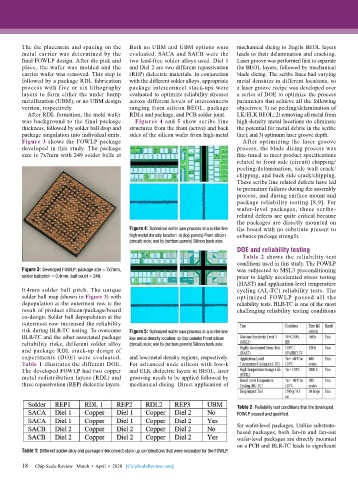
        Figure 3 shows the FOWLP package                                        After optimizing the laser groove
        developed in this study. The package                                  process, the blade dicing process was
        size is 7x7mm with 249 solder balls at                                fine-tuned to meet product specifications
                                                                              related to front side (circuit) chipping/
                                                                              peeling/delamination, side wall crack/
                                                                              chipping, and back side crack/chipping.
                                                                              These scribe line related defects have led
                                                                              to premature failures during the assembly
                                                                              process, and during surface mount and
                                                                              package reliability testing [8,9]. For
                                                                              wafer-level packages, these scribe-
                                                                              related defects are quite critical because
                                                                              the packages are directly mounted on
                                           Figure 4: Optimized wafer saw process at a scribe line   the board with no substrate present to
                                           high metal density location: a) (top panels) Front silicon   enhance package strength.
                                           (circuit) side; and b) (bottom panels) Silicon back side.
                                                                              DOE and reliability testing
                                                                                Table 2 shows the reliability test
                                                                              conditions used in this study. The FOWLP
        Figure 3: Developed FOWLP: package size = 7x7mm,                      was subjected to MSL3 preconditioning
        solder ball pitch = 0.4mm, ball count = 249.                          prior to highly accelerated stress testing
                                                                              (HAST) and application-level temperature
        0.4mm solder ball pitch. The unique                                   cycling (AL-TC) reliability tests. The
        solder ball map (shown in Figure 3) with                              optimized  FOWLP  passed  all  the
        depopulation at the outermost row is the                              reliability tests. BLR-TC is one of the most
        result of product silicon/package/board                               challenging reliability testing conditions
        co-design. Solder ball depopulation at the
        outermost row increased the reliability
        risk during BLR-TC testing. To overcome   Figure 5: Optimized wafer saw process at a scribe line
        BLR-TC and the other associated package   low metal density location: a) (top panels) Front silicon
        reliability risks, different solder alloy   (circuit) side; and b) (bottom panels) Silicon back side.
        and package RDL stack-up design of
        experiments (DOE) were evaluated.   and low-metal density regions, respectively.
        Table 1 illustrates the different DOE.   For advanced node silicon with low-k
        The developed FOWLP had two copper   and ELK dielectric layers in BEOL, laser
        metal redistribution layers (RDL) and   grooving needs to be applied followed by
        three repassivation (REP) dielectric layers.   mechanical dicing. Direct application of


                                                                              Table 2: Reliability test conditions that the developed
                                                                              FOWLP passed and qualified.
                                                                              for wafer-level packages. Unlike substrate-
                                                                              based packages, both fan-in and fan-out
                                                                              wafer-level packages are directly mounted
                                                                              on a PCB and BLR-TC leads to significant
        Table 1: Different solder alloy and package interconnect stack up combinations that were evaluated for the FOWLP.

        18
        18   Chip Scale Review   March  •  April  •  2020   [ChipScaleReview.com]

