Page 16 - ChipScale_Mar-Apr_2020-digital
P. 16
For other applications, the antenna could
                                                                              be an SiP module antenna or a flip-chip
                                                                              chip-scale package (fcCSP) with package
                                                                              on package (PoP) antenna. The different
                                                                              design options include: 1) SiP mmWave
                                                                              antenna module; 2) partial molding; 3)
                                                                              passive/filter integration; 4) array antenna
                                                                              design; and 5) small form factor.

        Figure 3: With an AiP design, the antenna is not a separate device, but is integrated in the device package.  Shielding
                                                                                For higher levels of system integration,
                                                                              a dva nc e d  Si P  a nd  R F  sh ield i ng
                                                                              technologies are employed. RF SiPs can
                                                                              contain the complete RF to base-band
                                                                              system functionality with an integrated
                                                                              antenna and antenna matching circuitry.
                                                                              The result is a fully-integrated AiP where
                                                                              all the elements of at least one complete
                                                                              RF system is included in the format of a
                                                                              single semiconductor package.
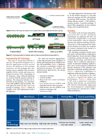
                                                                                RF shielding techniques include dual-
                                                                              side mold, conformal shield, compartment
        Figure 4: A technology toolbox for integrated antenna includes several different package platforms.  shield using laser trench and paste filling
        Implementing AiP technology          For some cost-sensitive applications,   technology, partial molding, selective
          The type of integrated antenna or   a flip-chip ball grid array (FCBGA) or   conformal shielding, and hybrid SiP
        specific AiP platform designed into a   double-sided ball grid array (DSBGA) are   designs. These techniques implement a
        specific application involves several   two AiP possibilities. Figure 4 illustrates   variety of materials including conductive
        factors. In addition to the antenna   the extensive technology toolbox for   lids, cored, coreless and low coefficient of
        structures, an AiP package may also   integrated antennas. For mobile and   thermal expansion (CTE) substrates and
        include a power amplifier (PA), low-noise   infrastructure applications, the design   innovative conformal shielding materials.
        amplifier (LNA), switch and transceiver   options include:            Figure 5 shows key technologies to
        integrated circuits (ICs). Depending on                               implement different shielding techniques.
        the frequency range, different platforms   •  Antenna in substrate;     The type  of shielding  in  the  AiP
        are used for both the antenna and the IC   •  Antenna module;         can have  a signif icant  impact  on
        package. The integrated antenna can be   •  Dual-side die mount packages   performance.  Figure 6 shows how
        mounted on the package, on a substrate,   (DSBGA);                    a SiP with a sputtered conformal
        or in a SiP mmWave antenna module. The   •  Low density fan-out (LDFO) with   shield outperforms an unshielded
        AiP approach itself can also vary from   integrated antenna layer substrate;  SiP, thereby substantially improving
        package to package. Figure 3 shows an   •  High-density fan-out (HDFO) with   the electromagnetic compatibility/
        example of an AiP implemented with a   antenna on package; and        electromagnetic interference (EMC/
        SiP approach.                        •  Antenna on mold.              EMI) performance.


        Figure 5: A variety of SiP RF shielding techniques address different design requirements.

        14   Chip Scale Review   March  •  April  •  2020   [ChipScaleReview.com]
        14

