Page 17 - ChipScale_Mar-Apr_2020-digital
P. 17
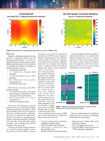
Figure 6: Near-field conformal shielding performance measurements from 100MHz to 6GHz.

        Materials                          designers and original equipment     Another design factor that can improve
          Similar to shielding, material selection   manufacturer (OEM) system designers.   antenna performance is to optimize the
        also has a significant impact on AiP   Design considerations for 5G substrates   substrate stack-up (see Figure 7). Direct
        design and performance—a variety of   must account for different package-  connection with receive/transmit (RX/
        materials provide design options to meet   level signal losses including: conductor,   TX) signals reduces signal mismatches
        different performance levels. In addition   dielectric loss, leakage and radiation   that can negatively impact the receiver
        to materials for mmWave shielding, an   losses. Conductor losses must address   signal sensitivity and increase power
        antenna substrate can have:        plating, skin depth, surface roughness,   consumption at the transmitter.
         •  Asymmetrical stack-up;         and via (str uct ure,
         •  <3.3 dielect r ic constant (Dk)   pitch and placement).
           materials;                      Key elements affecting
         •  <0.005 dissipation factor (Df )   dielectric loss include
           materials;                      the substrate materials’
         •  Ra >300nm (Cu trace surface    dissipation factor and
           roughness); and                 dielectric constant. The
         •  Low Dk/Df solder resist.       substrate materials’
                                           thick ness stack-up
          Wafer-level processing and LDFO   also has a direct effect
        packages include:                  on signal integrity
         •  Low Dk/Df passivation and mold/  (e.g., core, prepreg
           electromagnetic compatibility (EMC);  a n d  s o l d e r  m a s k
         •  Thick passivation development;  thickness). The epoxy
         •  Mu lt i-l aye r R DL fo r T-l i n e /  mold compound may
           waveguide; and                  also come into play for
         •  Wafer-level magnetic shield.   structures where the
                                           mold compound is used
          Advanced, high-frequency discrete   as a dielectric. Leakage
        antenna/transceiver applications employ   losses can occur within   Figure 7: Optimized substrate stack-up and RDL/via routing can improve
        wafer-level package technologies, where   the plane due to under-  antenna performance by reducing signal mismatch.
        the metal RDLs that form the antennas’   etched seed layers and
        elements are high precision, repeatable,   between substrate layers because of RDL   Specific implementations of different
        and easily tuned for the application.   and via patterning defects. Radiation   design aspects in a variety of packaging
        Specific AiP platform implementations   losses can occur because of:  technologies for AiP include:
        include: 1) Top layer assembly; 2) Double-
        side assembly; 3) Double-side molded   •  Circuit configuration: stripline,   •  Body sizes up to 23.0mm with several
        assembly; and 4) Double-side molded    complainer and microstrip;         form factor options;
        assembly with exposed die.           •  Via stub (radiation and reflection);  •  Up to 14 substrate layers; and
          Choosing the right package platform   •  I m p e d an c e  t r an s i t i o n  an d   •  Thin-film RDLs and dielectrics for
        for a specific design typically involves   discontinuities; and           77GHz and higher applications.
        discussions between OSAT package     •  Spurious resonance frequency spectra.


                                                                                                             15
                                                             Chip Scale Review   March  •  April  •  2020   [ChipScaleReview.com]  15

