Page 19 - ChipScale_Mar-Apr_2020-digital
P. 19
Advanced FOWLP for small form factor and


        high-performance microcontroller apps


        By Gaurav Sharma, Nishant Lakhera, Mollie Benson, Andrew J. Mawer  [NXP Semiconductors]
        O          ver the past few years, the   level temperature cycling (BLR-TC),   Fan-out package process


                   fan-out wafer-level package
                   (FOWLP) platform has    both fan-in and fan-out wafer-level   development
                                           packages have solder joint cracking
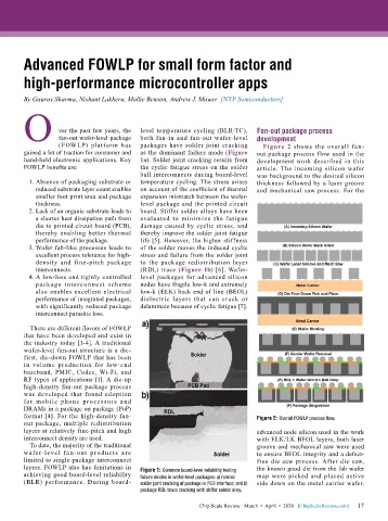
                                                                                Figure 2 shows the overall fan-
        gained a lot of traction for consumer and   as the dominant failure mode (Figure   out package process flow used in the
        hand-held electronic applications. Key   1a). Solder joint cracking results from   development work described in this
        FOWLP benefits are:                the cyclic fatigue stress on the solder   article. The incoming silicon wafer
                                           ball interconnects during board-level   was background to the desired silicon
          1. Absence of packaging substrate or   temperature cycling. The stress arises   thickness followed by a laser groove
            reduced substrate layer count enables   on account of the coefficient of thermal   and mechanical saw process. For the
            smaller foot print area and package   expansion mismatch between the wafer-
            thickness.                     level package and the printed circuit
          2. Lack of an organic substrate leads to   board. Stiffer solder alloys have been
            a shorter heat dissipation path from   evaluated  to  minimize  the fatigue
            die to printed circuit board (PCB),   damage caused by cyclic stress, and
            thereby enabling better thermal   thereby improve the solder joint fatigue
            performance of the package.    life [5]. However, the higher stiffness
          3. Wafer fab-like processes leads to   of the solder moves the induced cyclic
            excellent process tolerance for high-  stress and failure from the solder joint
            density and fine-pitch package   to the package redistribution layer
            interconnects.                 (RDL) trace (Figure 1b) [6]. Wafer-
          4. A low-loss and tightly controlled   level packages for advanced silicon
            package intercon nect scheme   nodes have fragile low-k and extremely
            also enables excellent electrical   low-k (ELK) back end of line (BEOL)
            performance of integrated packages,   dielectric layers that can crack or
            with significantly reduced package   delaminate because of cyclic fatigue [7].
            interconnect parasitic loss.

          There are different flavors of FOWLP
        that have been developed and exist in
        the industry today [1-4]. A traditional
        wafer-level fan-out structure is a die-
        first, die-down FOWLP that has been
        in volume production for low-end
        baseband, PMIC, Codec, Wi-Fi, and
        RF types of applications [1]. A die-up
        high-density fan-out package process
        was developed that found adoption
        for  mobile  phone  processors  and
        DRAMs in a package on package (PoP)
        format [4]. For the high-density fan-                                 Figure 2: Overall FOWLP process flow.
        out package, multiple redistribution
        layers at relatively fine-pitch and high                              advanced node silicon used in the work
        interconnect density are used.                                        with ELK/LK BEOL layers, both laser
          To date, the majority of the traditional                            groove and mechanical saw were used
        wafer-level fan-out products are                                      to ensure BEOL integrity and a defect-
        limited to single-package interconnect                                free die saw process. After die saw,
        layers. FOWLP also has limitations in   Figure 1: Common board-level reliability testing   the known good die from the fab wafer
        achieving good board-level reliability   failure modes in wafer-level packages: a) normal   map were picked and placed active
        (BLR) performance. During board-   solder joint cracking at package or PCB interface; and b)   side down on the metal carrier wafer.
                                           package RDL trace cracking with stiffer solder alloy.

                                                                                                             17
                                                             Chip Scale Review   March  •  April  •  2020   [ChipScaleReview.com]  17

