Page 12 - ChipScale_Mar-Apr_2020-digital
P. 12
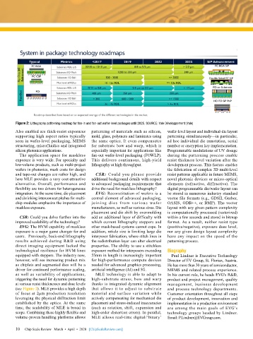
Figure 2: Lithography patterning roadmap for fan-in and fan-out wafer-level packages until 2025. SOURCE: Yole Développement (Yole)
        Also enabled are thick-resist exposures   patterning of materials such as silicon,   wafer-level layout and individual-die layout
        supporting high aspect ratios typically   mold, glass, polymers and laminates using   patterning simultaneously—in particular,
        seen in wafer-level packaging, MEMS   the same optics. It even compensates   ad hoc individual die annotation, serial
        structuring, microfluidics and integrated   for substrate bow and warp, which is   number or encryption key implementation.
        silicon photonics applications.    especially important for applications like   Programmable modulations of UV dosage
          The application space for maskless   fan-out wafer-level packaging (FOWLP).   during the patterning process enable
        exposure is very wide. For specialty and   This delivers continuous, high-yield   resist thickness level variation after the
        low-volume products, such as multi-project   lithography at high throughput.  development process. This feature enables
        wafers in photonics, mask costs for design                            the fabrication of complex 3D multi-level
        and tape-out changes are rather high, and   CSR: Could you please provide   resist patterns applicable in future MEMS,
        here MLE provides a very cost-attractive   additional background details with respect   novel photonic devices or micro-optical
        alternative. Overall, performance and   to advanced packaging requirements that   elements (refractive, diffractive). The
        flexibility are two drivers for heterogeneous   drive the need for maskless lithography?  digital programmable die/wafer layout can
        integration. At the same time, die placement   EVG: Reconstitution of wafers is a   be stored in numerous industry standard
        and shrinking interconnect pitches for multi-  central element of advanced packaging,   vector file formats (e.g., GDSII, Gerber,
        chip modules emphasize the importance of   joi n i ng dies f rom va r ious wafer   OASIS, ODB++, or BMP). The vector
        maskless exposure.                 manufacturers, as well as various sizes. Die   layout with any given pattern complexity
                                           placement and die shift by overmolding   is computationally processed (rasterized)
          CSR: Could you delve further into the   add an additional layer of difficulty with   within a few seconds and stored in bitmap
        improved scalability of the technology?   which current lithography steppers and   format. As a result, neither resist type
          EVG: The HVM capability of maskless   other mask-based systems cannot cope. In   (positive/negative), exposure dose level,
        exposure is a major game changer for end   addition, reticle size is limiting large die   nor any given design layout complexity
        users.  Previously, back-end lithography   interposer fabrication, where stitch lines in   have any impact on the speed of the
        results achieved during R&D using   the redistribution layer can alter electrical   patterning process.
        direct imaging equipment lacked the   properties. The ability to use a stitchless
        technological resilience for HVM lines   exposure method for interposers exceeding   Biography
        equipped with steppers. The industry now,   55mm in length is increasingly important   Paul Lindner is Executive Technology
        however, will see increasing product mix   for high-performance compute devices   Director of EV Group, St. Florian, Austria.
        as chiplets and segmented dies will be a   needed for advanced graphics processing,   He has more than 30 years of semiconductor,
        driver for continued performance scaling,   artificial intelligence (AI) and 5G.  MEMS and related process experience.
        as well as variability of applications,   MLE technology is able to adapt to   In his current role, he heads EVG’s R&D,
        triggering the need for dynamic patterning   high-substrate stress, bow and warp   product and project management, quality
        at various resist thicknesses and dose levels   thanks to integrated dynamic alignment   management, business development
        (see Figure 2). MLE provides a high depth   that allows it to adjust to substrate   and process technology departments.
        of focus at 2µm production resolution   material and surface variation while   Customer orientation throughout all steps
        leveraging the physical diffraction limit   actively compensating for mechanical die   of product development, innovation and
        established by the optics. At the same   placement and stress-induced inaccuracies   implementation in a production environment
        time, the scalability of MLE is broad in   (such as rotation, shift, expansion and   are among the main goals of EVG’s
        scope. Combining these highly flexible and   high-order distortion errors). In parallel,   technology groups headed by Lindner.
        volume-proven handling platforms allows   MLE allows real-time digital/‘binary’   Email: P.Lindner@EVGroup.com.

        10   Chip Scale Review   March  •  April  •  2020   [ChipScaleReview.com]
        10

