Page 8 - ChipScale_Mar-Apr_2020-digital
P. 8
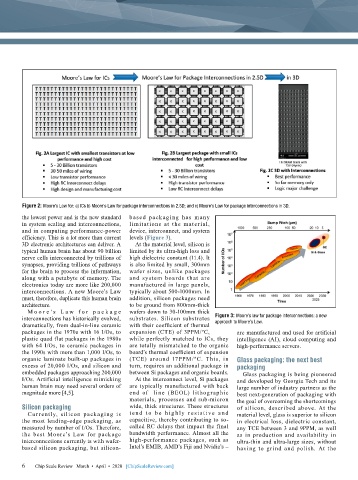
Figure 2: Moore’s Law for: a) ICs b) Moore’s Law for package interconnections in 2.5D; and c) Moore’s Law for package interconnections in 3D.

        the lowest power and is the new standard   based packaging has many
        in system scaling and interconnections,   limitations at  the  material,
        and in computing performance-power   device, interconnect, and system
        efficiency. This is a lot more than current   levels (Figure 3).
        3D electronic architectures can deliver. A   At the material level, silicon is
        typical human brain has about 90 billion   limited by its ultra-high loss and
        nerve cells interconnected by trillions of   high dielectric constant (11.4). It
        synapses, providing trillions of pathways   is also limited by small, 300mm
        for the brain to process the information,   wafer sizes, unlike packages
        along with a petabyte of memory. The   and system boards that are
        electronics today are more like 200,000   manufactured in large panels,
        interconnections. A new Moore’s Law   typically about 500-1000mm. In
        must, therefore, duplicate this human brain   addition, silicon packages need
        architecture.                      to be ground from 800mm-thick
          M o o r e ’ s L a w f o r p a c k a g e   wafers down to 30-100mm thick
        interconnections has historically evolved,   substrates. Silicon substrates   Figure 3: Moore’s law for package interconnections: a new
        dramatically, from dual-in-line ceramic   with their coefficient of thermal   approach to Moore’s Law.
        packages in the 1970s with 16 I/Os, to   expansion (CTE) of 3PPM/ºC,   are manufactured and used for artificial
        plastic quad flat packages in the 1980s   while perfectly matched to ICs, they   intelligence (AI), cloud computing and
        with 64 I/Os, to ceramic packages in   are totally mismatched to the organic   high-performance servers.
        the 1990s with more than 1,000 I/Os, to   board’s thermal coefficient of expansion
        organic laminate built-up packages in   (TCE) around 17PPM/ºC. This, in   Glass packaging: the next best
        excess of 20,000 I/Os, and silicon and   turn, requires an additional package in   packaging
        embedded packages approaching 200,000   between Si packages and organic boards.  Glass packaging is being pioneered
        I/Os. Artificial intelligence mimicking   At the interconnect level, Si packages   and developed by Georgia Tech and its
        human brain may need several orders of   are typically manufactured with back   large number of industry partners as the
        magnitude more [4,5].              end of  line (BEOL) lithographic   best next-generation of packaging with
                                           materials, processes and sub-micron   the goal of overcoming the shortcomings
        Silicon packaging                  wide, thick structures. These structures   of silicon, described above. At the
          Cur rently, silicon packaging is   t e nd t o b e h ig h ly r e si s t ive a nd   material level, glass is superior to silicon
        the most leading-edge packaging, as   capacitive, thereby contributing to so-  in electrical loss, dielectric constant,
        measured by number of I/Os. Therefore,   called RC delays that impact the final   any TCE between 3 and 9PPM, as well
        the best Moore’s Law for package   bandwidth performance. Almost all the   as in production and availability in
        interconnections currently is with wafer-  high-performance packages, such as   ultra-thin and ultra-large sizes, without
        based silicon packaging, but silicon-  Intel’s EMIB, AMD’s Fiji and Nvidia’s –   having to grind and polish. At the


        6 6  Chip Scale Review   March  •  April  •  2020   [ChipScaleReview.com]

