Page 11 - ChipScale_Mar-Apr_2020-digital
P. 11
TECHNOLOGY TRENDS


                           EV Group takes on maskless lithography for


                           MEMS and advanced packaging


                           CSR asked Paul Lindner, Executive Technology Director at EV Group, to comment on the company’s
                           developments in maskless lithography.


          CSR: EVG is using maskless lithography   in lithography triggered our development   wafers in advanced packaging, where epoxy
        to address future back-end lithography   of the maskless exposure technology   materials or carrier-mounted thin wafers for
        needs for advanced packaging and   (MLE™) to meet critical requirements of   interposers add up to several millimeters of
        microelectromechanical systems (MEMS),   design flexibility and minimal development   bowing and warp variation. Handling such
        among other applications. What is it about   cycles in the high-volume-manufacturing   wafers needs adaptable equipment handling
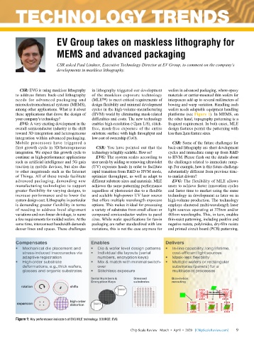
        these applications that drove the design of   (HVM) world by eliminating mask-related   platforms (see Figure 1). In MEMS, on
        your company’s technology?         difficulties and costs. The new technology   the other hand, topography patterning is a
          EVG: A very exciting development in the   enables high-resolution (<2µm L/S), stitch-  frequent requirement. In both cases, MLE
        overall semiconductor industry is the shift   free, mask-free exposure of the entire   design features permit the patterning with
        toward 3D integration and heterogeneous   substrate surface with high throughput and   less than 2µm feature sizes.
        integration within advanced packaging.   low cost of ownership (CoO).
        Mobile processors have triggered a                                      CSR: Some of the future challenges for
        first growth cycle in 3D/heterogeneous   CSR: You have pointed out that the   back-end lithography are short development
        integration. We expect this growth cycle to   technology is highly scalable. How so?  cycles and immediate ramp up from R&D
        continue as high-performance applications   EVG: The system scales according to   to HVM. Please flesh out the details about
        such as artificial intelligence and 5G gain   user needs by adding or removing ultraviolet   the challenges related to immediate ramp-
        traction in mobile devices, but also due   (UV) exposure heads in order to facilitate   up. For example, how is this future challenge
        to other megatrends such as the Internet   rapid transition from R&D to HVM mode,   substantially different from previous time-
        of Things. All of these trends facilitate   optimize throughput, as well as adapt to   to-market drivers?
        advanced packaging, demanding new   different substrate sizes and materials. MLE   EVG: The flexibility of MLE allows
        manufacturing technologies to support   achieves the same patterning performance   users to achieve faster innovation cycles
        greater flexibility for varying designs, to   regardless of photoresist due to a flexible   and faster time to market using the same
        increase performance and to lower the   and scalable high-power UV laser source   technology in development as later on in
        system design cost. Lithography in particular   that offers multiple wavelength exposure   high-volume production. The technology
        is demanding greater flexibility in terms   options. This makes it ideal for processing   employs clustered multi-wavelength laser
        of needing to address local alignment   a variety of substrates from small silicon or   light sources operating at 375nm and/or
        variations and non-linear shrinkage, to name   compound semiconductor wafers to panel   405nm wavelengths. This, in turn, enables
        a few requirements for molded wafers. At the   sizes. While wafer specifications for fan-in   thin-resist patterning, including positive and
        same time, interconnect bandwidth demands   packaging are rather standardized with low   negative resists, polyimides, dry-film resists
        denser lines and spaces. These challenges   variations, this is not the case anymore for   and printed circuit board (PCB) patterning.


        Figure 1: Key performance indicators of EVG MLE technology. SOURCE: EVG

                                                             Chip Scale Review   March  •  April  •  2020   [ChipScaleReview.com]  9 9

