Page 38 - ChipScale_Mar-Apr_2020-digital
P. 38
Navigating dicing on increasing complex shrinking die


        By M. Todd Wyant  [Texas Instruments]
        I     n semiconductor manufacturing,   generation of silicon semiconductor   out for a typical device produced. The


              all circuits are placed onto the
                                           on the fabrication alignment used
              wafer  with  an  applied  street   products. Typically, this is dependent   entire map shows how the stepper is
                                                                              used to layout the wafer for maximum
        width between component structures,   a nd is ge ne r a l ly det e r m i ne d by   efficiency of the equipment utilized
        enabling a process that cuts the wafers   alignment among equipment vendors to   to align and build products. These
        into individual pieces following wafer   maximize process capabilities. In most   structures are critical to fabrication
        fabrication processes. After spending so   cases, back up patterns and multiple   wafer-to-shot alignment capabilities and
        much time and effort creating complex   placements are performed to enable   necessary to enable production in high-
        and challenging circuits, it can be   alignment stability over the course of   volume manufacturing. The structures
        frustrating that the first processing step   time and compensate for manufacturing   are typically composed of metal build ups
        during assembly uses various techniques   and  equipment  variability  in  wafer   shown in Figure 2.
        to singulate individual circuits, as those   fabrication areas.         These structures consist of via and
        steps can create potential damage to such   Figure 1 shows an example shot   solid metal covers comprised of each
        delicate circuits. Nonetheless, mechanical   map, and the red box locations show the   of the individual fabrication layers,
        dicing of wafers has been the process of   estimated alignment locations as laid   with up to six metal thickness layers
        record for many years. Mechanical dicing
        utilizes a high-speed diamond blade
        to remove unwanted silicon between
        circuits. This diamond blade can be
        adjusted and changed to meet many
        differences with silicon technologies,
        metal densities and configurations.
          Mechanical dicing has long been a
        significant challenging manufacturing
        process step for any semiconductor
        operation. Mounting pressures to push
        die per wafer increases, in an effort to
        lower costs, create a situation where
        narrow scribes in a growing complexity
        of devices is normal. These increasing
        improvements also require the same
        quality levels within the fracturing
        location. This shifting complexity
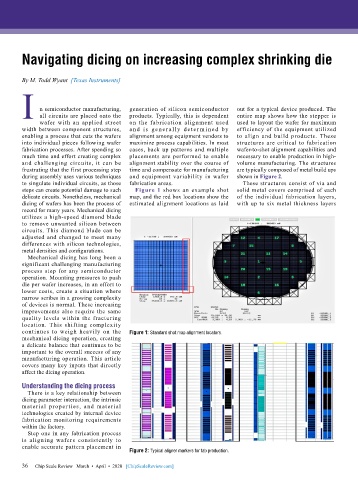
        continues to weigh heavily on the   Figure 1: Standard shot map alignment locators.
        mechanical dicing operation, creating
        a delicate balance that continues to be
        important to the overall success of any
        manufacturing operation. This article
        covers many key inputs that directly
        affect the dicing operation.

        Understanding the dicing process
          There is a key relationship between
        dicing parameter interaction, the intrinsic
        material properties, and material
        technologies created by internal device
        fabrication monitoring requirements
        within the factory.
          Step one in any fabrication process
        is aligning wafers consistently to
        enable accurate pattern placement in
                                           Figure 2: Typical aligner markers for fab production.

        36
        36   Chip Scale Review   March  •  April  •  2020   [ChipScaleReview.com]

