Page 40 - ChipScale_Mar-Apr_2020-digital
P. 40
the test pads and wafer fabrications
                                                                              features into a subset of the wafer.
                                                                              Blading enables a die loss and product
                                                                              cost increase, but eliminates many
                                                                              modules from  the dicing streets.
                                                                              Removing the modules creates a
                                                                              clean area for cutting and loading that
                                                                              improves problems associated with
                                                                              mechanical dicing. There are other
                                                                              complications that interact, such as
                                                                              films  used,  and  wire  bond  versus  a
                                                                              bumped device, but the major items
                                                                              discussed here are the driving reasons
                                                                              for mechanical dicing complications.

                                                                              Packaging requirements and
                                                                              interactions
                                                                                Now that we have covered wafer fab
                                                                              complications, let’s now move on to
        Figure 3: Probe pad example.                                          packaging requirements and interactions,
                                                                              wafer dicing challenges associated with
                                                                              package type, and finally, interaction
                                                                              with scribe structures that need to be
                                                                              considered during the design phase.
                                                                                For example, if your device is for the
                                                                              automotive market, you should consider
                                                                              asking the following questions: Does it
                                                                              have burn-in? Is the package prone to high
                                                                              stress? Knowing your end customer’s
                                                                              requirements and asking these questions
                                                                              are normally  considered during a design
                                                                              phase review. However, many times parts
                                                                              are multi-purposed and can be sold across
                                                                              many different package types, families and
                                                                              end user types. This situation complicates
                                                                              the process further. Don’t panic if you are
        Figure 4: Die size interaction to open streets.
                                                                              a dicing engineer. The daily challenge
        Driving improvements                 Another option is to utilize die   of the job is to review in advance and
          As die sizes shrink, improvements   drop-in reticle shots. This is counter   predict metal density capabilities, and then
        in structure layout and placement can   intuitive in the wafer fabrication area,   adjust and work to solve complex dicing
        enable improvements in dicing and   as it incorporates complex techniques,   challenges prior to them happening.
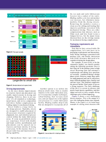
        chipping. However, there is not one   called blading, that increase mask   Figure 5 shows a very challenging
        rule—it’s all standard as technology,   cost, and can impact one or the highest   dicing situation. This is the output of a
        metal layers, and device composition   cost processes in a wafer fabrication   new and challenging design type released.
        will driver further complications on   facility. Blading enables drop-in die   Shown in the figure is a six metal layer
        loading impact to mechanical dicing.  that are designed to incorporate all of   example of a dicing street structure with
          Street width is a large factor in
        the design process. Typically, streets
        are designed to enable placement of
        all necessary structures required for
        alignment, test, and statistical process
        control within the wafer fabrication
        areas. If room on prohibited streets
        are sometimes f itted with  double
        and triple scribes, metallization and
        placements can be spaced out to
        improve and lower density of dicing
        street areas. In this manner, there is a
        die per wafer loss and improvement in
        dicing capability.                 Figure 5: Cross section of 6-metal layer device.

        38
        38   Chip Scale Review   March  •  April  •  2020   [ChipScaleReview.com]

