Page 44 - ChipScale_Mar-Apr_2020-digital
P. 44
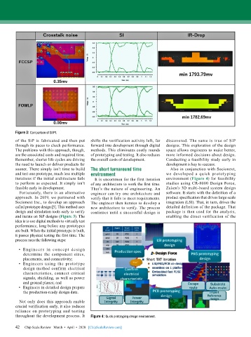
Figure 3: Comparison of SI/PI.
        of the SiP is fabricated and then put   shifts the verification activity left, far   discovered. The same is true of SiP
        through its paces to check performance.   forward into development through digital   designs. This exploration of the design
        The problems with this approach, though,   methods. This eliminates costly rounds   space allows engineers to make better,
        are the associated costs and required time.   of prototyping and testing. It also reduces   more informed decisions about design.
        Remember, shorter life cycles are driving   the overall costs of development.  Conducting a feasibility study early in
        the need to launch or deliver products far                            development is key to success.
        sooner. There simply isn’t time to build   The short turnaround time    Also in conjunction with Socionext,
        and test one prototype, much less multiple   environment              we developed a quick prototyping
        iterations if the initial architecture fails   It is uncommon for the first iteration   environment (Figure 4) for feasibility
        to perform as expected. It simply isn’t   of any architecture to work the first time.   studies using CR-8000 Design Force,
        feasible early in development.     That’s the nature of engineering. An   Zuken’s 3D multi-board system design
          Fortunately, there is an alternative   engineer can try one architecture and   software. It starts with the definition of a
        approach. In 2019, we partnered with   verify that it fails to meet requirements.   product specification that drives large scale
        Socionext Inc., to develop an approach   The engineer then iterates to develop a   integration (LSI). That, in turn, drives the
        called prototype design [5]. This method uses   new architecture to verify. The process   detailed definition of the package. That
        design and simulation tools early to verify   continues until a successful design is   package is then used for the analysis,
        and iterate on SiP designs (Figure 3). The                            enabling the direct verification of the
        idea is to use digital methods to virtually test
        performance, long before any prototypes
        are built. When the initial prototype is built,
        it passes physical testing the first time. The
        process uses the following steps:

          •  Eng i neers  i n  concept  desig n
            determine the component sizes,
            placements, and connectivity;
          •  Engineers using the prototype
            design method confirm electrical
            characteristics, connect critical
            signals, shielding, as well as power
            and ground planes; and
          •  Engineers in detailed design prepare
            the production-ready design data.

          Not only does this approach enable
        crucial verification early, it also reduces
        reliance  on prototyping and testing
        throughout the development process. It   Figure 4: Quick prototyping design environment.

        42
        42   Chip Scale Review   March  •  April  •  2020   [ChipScaleReview.com]

