Page 49 - ChipScale_Mar-Apr_2020-digital
P. 49
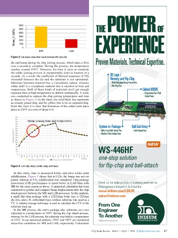
Figure 3: Die stress simulation result between MR and LAB.
        die and bump during the chip joining process, which takes a little
        over a second to complete. During the process, the temperature
        reaches around 230ºC. However, the time it takes to complete
        the solder joining process is exceptionally short (a fraction of a
        second). As a result, the coefficient of thermal expansion (CTE)   • 3D Logic /
        mismatch between the die and the substrate is not substantial.       Memory and Flip-Chip
        Substrate laminate material has a viscoelastic nature, whereas   – Wafer Bumping (Bump Fusion) Flux
        solder itself is a viscoplastic material that is sensitive to time and   – Flip-Chip Flux
        temperature. Both of these kinds of materials don’t get enough                       • Lidded MEMS
        exposure time at high temperature to deform inelastically. A study                     – Dispensable Fine-Pitch
        was conducted to capture the chip joining temperature and time                             Solder Paste
        as shown in Figure 4. In the chart, the solid black line represents
        an already joined chip, and the yellow line is for an unjoined chip.                     Wafer-Level Package
        From the chart it is clear that formation of the solder joint takes                      Ultra-Small Passive
        place at 230ºC at a time of about 0.3s.


                                                                  System-in-Package •   Ball Grid Array •
                                                                  – Wafer Level Ball-Attach Flux  – Ball-Attach Flux
                                                                  – Ultrafine-Pitch Solder Paste


                                                                                                  NEW
                                                                  WS-446HF


                                                                  one-stop solution

                                                                  for flip-chip and ball-attach
        Figure 4: LAB chip attach profile using an IR laser.
          In this study, time is measured before and after solder joint
        solidification. Figure 5 shows that at 0.25s, the bump was not yet
        joined, whereas at 0.3s, solidification was completed. Chip-package
        interaction (CPI) performance is much better in LAB than with   Check out our wide portfolio of soldering materials for
        MR for the same reason as above. A numerical calculation has been   Heterogeneous Integration & Assembly:
        conducted to predict and compare bump displacement after the chip   www.indium.com/CSR/HI
        attach process between the MR and LAB processes. In this analysis,
        a small flip-chip package with a 12X12mm body size, a 5X5mm   askus@indium.com
        die size, and a 4L embedded trace coreless substrate was used as a
        TV. A volume average technique is used to calculate the CTE of the
        substrate stack up.
          In the MR process, the entire package (die, substrate, etc.) was
        subjected to a temperature of 220ºC during the chip attach process,
        whereas for the LAB process, the substrate was held to a temperature
        of 145ºC. In our numerical analysis, 220ºC and 145ºC are considered
        stress-free conditions for MR and LAB, respectively. Calculation

                                                                                                             47
                                                             Chip Scale Review   March  •  April  •  2020   [ChipScaleReview.com]  47

