Page 52 - ChipScale_Mar-Apr_2020-digital
P. 52

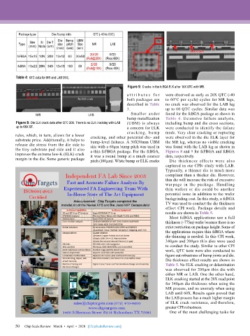
Table 4: QTC data for MR and LAB DOE.

                                                             Figure 9: Cracks in the fcBGA ELK after 10X QTC with MR.
                                                            a t t r i bu t e s f o r   were observed as early as 20X QTC (-40
                                                            both packages are   to 60ºC per cycle) cycles for MR legs,
                                                            described in Table   no crack was observed for the LAB leg
                                                            3.                up to 60 QTC cycles. Similar data was
                                                              Smaller under   found for the fcBGA package as shown in
                                                            bump metallization   Table 4. Extensive failure analysis,
         Figure 8: Die ELK crack data after QTC 20X. There is no ELK cracking with LAB   (UBM) is always   including bump and die cross sections,
         up to 60X QT.                                      a concern for ELK   were conducted to identify the failure
                                                            crack ing, bu mp   mode. Very clear cracking or rupturing
        rules, which, in turn, allows for a lower   cracking, and other potential die- and   were observed in the die ELK layer for
        substrate price. Additionally, it helps to   bump-level failures. A 30X50mm UBM   the MR leg, whereas no visible cracking
        release die stress from the die side to   size with a 60µm bump pitch was used in   was found with the LAB leg as shown in
        the tiny substrate pad side and it also   a thin fcFBGA package. For the fcBGA,   Figures 8 and 9 for fcFBGA and fcBGA
        improves the extreme low-K (ELK) crack   it was a round bump at a much coarser   data, respectively.
        margin in the die. Some generic package   pitch (180µm). White bump or ELK cracks   Die thickness effects were also
                                                                              captured in our CPIv study with LAB.
                                                                              Typically, a thinner die is much more
                                                                              compliant than a thicker die. However,
                                                                              thin die will increase the risk of excessive
                                                                              warpage in the package. Handling
                                                                              thin wafers or die could be another
                                                                              potential issue in addition to the wafer
                                                                              backgrinding cost. In this study, a fcBGA
                                                                              TV was used to conduct the die thickness
                                                                              effect CPI work. Package details and
                                                                              results are shown in Table 5.
                                                                                Most fcBGA applications use a full
                                                                              thickness (~775m) wafer because there is no
                                                                              strict restriction on package height. Some of
                                                                              the applications require thin fcBGA where
                                                                              die thinning is needed. In this CPI work,
                                                                              340µm and 200µm thin dies were used
                                                                              to conduct the study. Similar to other CPI
                                                                              work, QTC tests were also conducted to
                                                                              figure out robustness of bump joints and die.
                                                                              Die thickness effect results are shown in
                                                                              Table 5. No ELK cracking or delamination
                                                                              was observed for 200µm thin die with
                                                                              either MR or LAB. One the other hand,
                                                                              ELK cracking started at the 20X read point
                                                                              for 340µm die thickness when using the
                                                                              MR process, and no anomaly when using
                                                                              LAB until 60X. Results again proved that
                                                                              the LAB process has a much higher margin
                                                                              of ELK crack resistance, and therefore,
                                                                              greater CPI robustness.
                                                                                One of the most challenging tasks for


        50
        50   Chip Scale Review   March  •  April  •  2020   [ChipScaleReview.com]
   47   48   49   50   51   52   53   54   55   56   57