Page 53 - ChipScale_Mar-Apr_2020-digital
P. 53
the MR process is to attach fine-pitch die   associated with the new
        with a small under bump metallization   technology to overcome
        (UBM) bump. It experiences very high   assembly-related yields.
        stress from the CTE mismatch between   S t a n d a r d M R , T C B ,
        die and substrate. A typical failure mode   a n d t h e l a t e s t L A B
        for a small UBM bump is delamination   attach technologies were
        or UBM cracking. Using LAB, we     described in this paper.
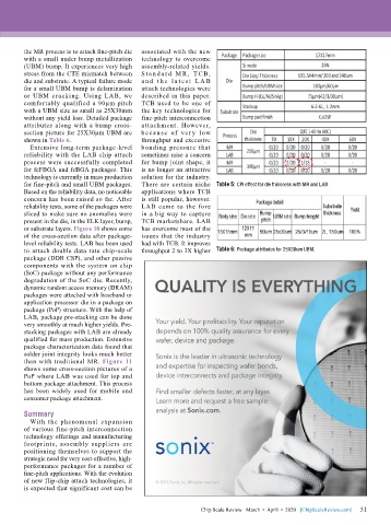
        comfortably qualified a 90µm pitch   TCB used to be one of
        with a UBM size as small as 25X30mm   the key technologies for
        without any yield loss. Detailed package   fine-pitch interconnection
        attributes along with a bump cross-  attachment. However,
        section picture for 25X30µm UBM are   b e cau se of ve r y low
        shown in Table 6.                  throughput and excessive
          Extensive long-term package-level   bonding pressure that
        reliability with the LAB chip attach   sometimes raise a concern
        process were successfully completed   for bump joint shape, it
        for fcFBGA and fcBGA packages. This   is no longer an attractive
        technology is currently in mass production   solution for the industry.
        for fine-pitch and small UBM packages.   There are certain niche  Table 5: CPI effect for die thickness with MR and LAB.
        Based on the reliability data, no noticeable   applications where TCB
        concern has been raised so far. After   is still popular, however.
        reliability tests, some of the packages were   LAB came to the fore
        sliced to make sure no anomalies were   in a big way to capture
        present in the die, in the ELK layer, bump,   TCB marketshare. LAB
        or substrate layers. Figure 10 shows some   has overcome most of the
        of the cross-section data after package-  issues that the industry
        level reliability tests. LAB has been used   had with TCB. It improves
        to attach double data rate chip-scale   throughput 2 to 3X higher   Table 6: Package attributes for 25X30um UBM.
        package (DDR CSP), and other passive
        components with the system on chip
        (SoC) package without any performance
        degradation of the SoC die. Recently,
        dynamic random access memory (DRAM)
        packages were attached with baseband or
        application processor die in a package on
        package (PoP) structure. With the help of
        LAB, package pre-stacking can be done
        very smoothly at much higher yields. Pre-
        stacking packages with LAB are already
        qualified for mass production. Extensive
        package characterization data found that
        solder joint integrity looks much better
        than with traditional MR. Figure 11
        shows some cross-section pictures of a
        PoP where LAB was used for top and
        bottom package attachment. This process
        has been widely used for mobile and
        consumer package attachment.

        Summary
          With the phenomenal  expansion
        of various fine-pitch interconnection
        technology offerings and manufacturing
        footprints, assembly suppliers are
        positioning themselves to support the
        strategic need for very cost-effective, high-
        performance packages for a number of
        fine-pitch applications. With the evolution
        of new flip-chip attach technologies, it
        is expected that significant cost can be


                                                                                                             51
                                                             Chip Scale Review   March  •  April  •  2020   [ChipScaleReview.com]  51

