Page 50 - ChipScale_Mar-Apr_2020-digital
P. 50
Process characterization: design
                                                                              of experiments
                                                                                Since early 2016, numerous studies
                                                                              have been conducted on actual packages
                                                                              to makes sure that LAB data does
                                                                              indeed indicate a substantial benefit
                                                                              over standard MR and TCB processes
                                                                              before ramping into mass production.
                                                                              In terms of the assembly process, there
                                                                              is no difference between MR and LAB
                                                                              except that the MR reflow process is
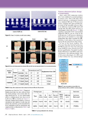
                                                                              interchanged with LAB (Figure 7). Both
                                                                              capillary underfill (CUF) and molded
                                                                              underfill (MUF) can be used in the
        Figure 5: IR laser time before and after solder joining.              LAB process. LAB process substrates
                                                                              don’t need to be heated to a very high
                                                                              temperature like what is needed for MR,
                                                                              therefore, it only takes a few seconds to
                                                                              heat up the die and perform chip joining.
                                                                                In one of the early studies, two
                                                                              TVs (one flip-chip fine-ball grid array
                                                                              [fcFBGA] and one flip-chip ball grid
                                                                              array [fcBGA]) were selected for LAB
                                                                              process qualification. Fine-pitch Cu pillar
                                                                              bump with bond on lead (BOL) pads were
                                                                              introduced in the substrate design. One
                                                                              of the great advantages of a BOL pad
                                                                              is that it allows for very relaxed design


        Figure 6: Bump joint displacement data between MR and LAB. Data are measured at die left, center, and right locations.


                                                                              Figure 7: Typical assembly process difference
        Table 2: Bump offset /displacement data comparison between MR and LAB processes.  between MR and LAB for a fcFBGA molded package.
        predictions are listed in Table 2. Empirical
        displacement data was also collected from
        the actual package cross section after the
        chip attach process. A very small bump
        offset or displacement was observed in
        LAB over MR as shown in Figure 6.
        Absolute displacement numbers between
        calculations and empirical results may not
        match, but trend wise, good correlation has
        been established between calculations and
        empirical data as illustrated in Table 2 and
        Figures 5 and 6.
                                           Table 3: TV package attributes for the LAB study.

        48
        48   Chip Scale Review   March  •  April  •  2020   [ChipScaleReview.com]

