Page 47 - ChipScale_Mar-Apr_2020-digital
P. 47
Laser-assisted bonding for fine-pitch cost-effective


        interconnection


        By Nokibul Islam, KyungOe Kim, Chris Scanlan, Choon Heung Lee  [JCET Group]
        A         dvanced semiconductor    the chips with the substrate. Because of   attractive alternative to overcome these


                  packaging requirements
                  f o r  h i g h e r  a n d  f a s t e r   the very fast process thermal budget and   issues. In this process, thermal energy
                                                                              from the infra-red (IR) laser heats up
                                           materials, thermal expansion mismatch
        performance in a thinner and smaller   is much lower than with MR or TCB,   the die and makes the joint between
        form factor continue to grow for mobile,   which results in less package warpage and   the die and substrate using a fine
        network, high-performance computing   less die-level stress. However, the laser   interconnection. With Cu pillar, it melts
        (HPC), and consumer devices. The   scanning length of LAB is still limited to   the solder cap and makes the joints with
        advanced node of the Si wafer drives   a certain size. As a result, throughput is   the substrate pad.  The laser beam used
        f ine-pitch bumping processes. A   about half that of MR, but compared to   for this process is similar to the die size
        significant reduction of the bump pitch   TCB, it is 2 to 3X higher. In this paper the   so the entire die can be heated up in
        has been observed over the last few   pros and cons of various package assembly   one shot of a laser scan. A typical LAB
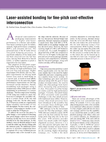
        years, moving from 40nm Si to 5nm Si   processes and comprehensive reliability   schematic process is shown in Figure 1.
        wafers. A further reduction in pitch is   data for fine-pitch packages, along with
        expected in the near future.       relative cost data, will be discussed.
          The adoption of fine-pitch copper
        (Cu) pillar bump has been growing as   Introduction
        the solution for high-performance and   Chip interconnection pitch has scaled
        low-cost flip-chip packages. Higher   down significantly over the last few
        input/output (I/O) density and very fine-  years mainly due to the need for higher
        pitch requirements are driving small   bandwidth and more computing power
        feature sizes such as small bump on   in a smaller form factor system. As
        a narrow pad, or bond-on-lead (BOL)   chip technology gets more and more
        interconnection. At the same time, higher   advanced along with the goal of more
        performance requirements are driving   product miniaturization, the need to
        increased current densities, thereby   reduce the chip package form factor
        assembling such packages using a   while increasing chip performance
        standard mass reflow (MR) process while   is clear. Fine-pitch Cu pillar bumps   Figure 1: LAB chip bonding process. COURTESY:
        maintaining its performance is a serious   are widely used for high-performance   link.springger.com
        challenge. Thermocompression bonding   packages. Certainly, fine-pitch bumps
        (TCB) using non-conductive paste has   do  often  encounter  some  assembly
        been used to mitigate the assembly risk,   challenges in the chip attach process   LAB pros and cons
        up to a certain extent, of die size and   with traditional mass reflow. However,   There are various advantages of the
        package body size. On the other hand,   various chip attach processes have   LAB process over conventional mass
        the TCB process results in a significantly   been introduced in the assembly line   reflow, for example: 1) it is a very quick
        higher assembly cost because of very   to overcome these challenges with   chip joining process (only a few seconds);
        low throughput. For this reason, the cost-  advanced Si nodes (≤14nm or 7nm).  2) no additional reflow process is needed;
        sensitive semiconductor market is not   MR continues to be the mainstream   3) it has a higher yield with less die stress
        ready to adopt the TCB process.    process for flip-chip packages, while   and warpage; and 4) it has the capability
          To address the need for fine-pitch Cu   TCB with non-conductive paste (NCP)   to use a much finer pitch, as well as a thin
        pillar bumps, a new method of attaching   used to be the best solution for finer   platform package with either a thin core
        fine-pitch bumps called laser-assisted   bump  pitch  flip-chip  die  in  the  last   or a coreless substrate, etc. Detailed pros
        bonding (LAB) has been successfully   few years. TCB certainly provides   and cons among MR, TCB, and LAB are
        introduced in flip-chip packages. In this   better chip attach yields with higher   listed in Table 1. Some may raise concern
        method, a laser (as thermal energy) is used   alignment accuracy, however it is a   for the power density of the LAB process.
                                                                                                        2
        to melt the solder cap, thereby joining with   very slow process and quite often the   Typically, a 300 to 500W/cm  power
        the substrate pads. No additional reflow   bump shape becomes an issue because   density is used in the process, which is
        process or excessive compression force   of excessive bond force. Other issues   much lower than what is used in a plasma
        is required. It’s a very localized process   are die cracking, higher die/package   marking process or an evaporation
        and requires only a few seconds to join   wa r page, etc.— LA B is the most   process, so device-level functionality is


                                                                                                             45
                                                             Chip Scale Review   March  •  April  •  2020   [ChipScaleReview.com]  45

