Page 54 - ChipScale_Mar-Apr_2020-digital
P. 54

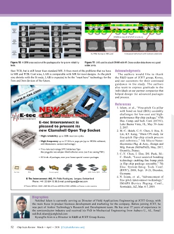
Figure 10: A SEM cross section of the packages after long-term reliability   Figure 11: LAB used to attach DRAM with AP. Cross-section data shows very good
        tests.                                            solder joints.
        than TCB, but is still lower than standard MR. It fixes most of the problems that we have   Acknowledgments
        in MR and TCB. Cost wise, LAB is comparable with MR for most designs. As the pitch   The authors would like to thank
        size shrinks with the Si node, LAB is expected to be the “must have” technology for the   the R&D team of JCET group, Korea,
        5nm and 3nm devices of the future.                                    and our customers for their continued
                                                                              guidance in the study. The authors
                                                                              also want to express gratitude to the
                                                                              individuals at our partner companies that
                                                                              helped design the advanced packages
                                                                              and process.

                                                                              References
                                                                                1. Islam, et al., “Fine-pitch Cu pillar
                                                                                  with bond on lead (BOL) assembly
                                                                                  challenges for low-cost and high-
                                                                                  performance flip-chip package,” 67th
                                                                                  Elec. Comp. and Tech. Conf. (ECTC),
                                                                                  Lake Buena Vista, FL, May 30–June
                                                                                  2, 2017.
                                                                                2. M.-C. Hsieh, C.-Y. Chen, I. Hsu, S.
                                                                                  Lin, KT. Kang, “10nm CPI study for
                                                                                  fine-pitch flip-chip attach process
                                                                                  and substrate,” 5th Micro/Nano-
                                                                                  Electronics Pkg. & Assy., Design and
                                                                                  Mfg. Forum (MiNaPAD), May, 2017,
                                                                                  Grenoble, France.
                                                                                3. C.-Y. Chen, I. Hsu, DS. Park, M.-
                                                                                  C. Hsieh, “Laser-assisted bonding
                                                                                  technology enabling fine bump pitch
                                                                                  in flip-chip package assembly,” 7th
                                                                                  Elec. System-Integ. Tech. Conf.
                                                                                  (ESTC), 2018, Sept. 18-21, Dresden,
                                                                                  Germany.
                                                                                4. N. Islam, et  al., “Advancement of
                   E-Tec Interconnect  AG, Mr. Pablo Rodriguez,  Lengnau Switzerland  fine-pitch interconnect technology,”
                       Phone : +41 32 654 15 50, E-mail: p.rodriguez@e-tec.com
                                                                                  IMAPS  Device  Pkging. Conf.,
                                                                                  Scottsdale, AZ, Mar. 4-7, 2019.


                       Biographies
                         Nokibul Islam is currently serving as Director of Field Applications Engineering at JCET Group, with
                       the main focus in product business development and marketing for the company. Before joining JCET, he
                       was part of Amkor Technology’s Research and Development team. He has over 17 years of experience in
                       the semiconductor industry and received his PhD in Mechanical Engineering from Auburn U., AL. Email
                       nokibul.islam@jcetglobal.com
                         KyungOe Kim is a Director in R&D at JCET Group Korea.


        52
        52   Chip Scale Review   March  •  April  •  2020   [ChipScaleReview.com]
   49   50   51   52   53   54   55   56   57   58   59