Page 53 - ChipScale_Jan-Feb_2021-digital
P. 53
structures (Figure 1c), by applying a full
        dose at the via and a partial dose for the
        redistribution layer (RDL) lines, a single-
        exposure process is used without impacting
        throughput. The inherent flexibility of
        maskless exposure, in conjunction with
        the light valve’s ability to modulate the
        exposure dose can reduce the number of
        process steps required and increase yield
        while maintaining throughput.

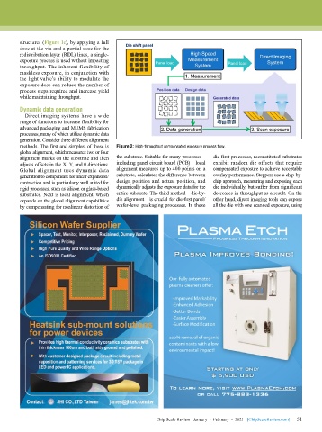
        Dynamic data generation
          Direct imaging systems have a wide
        range of functions to increase flexibility for
        advanced packaging and MEMS fabrication
        processes, many of which utilize dynamic data
        generation. Consider three different alignment
        methods. The first and simplest of these is   Figure 2: High-throughput compensated exposure process flow.
        global alignment, which measures two or four
        alignment marks on the substrate and then   the substrate. Suitable for many processes –   die-first processes, reconstituted substrates
        adjusts offsets in the X, Y, and θ directions.   including panel circuit board (PCB) – local   exhibit random die offsets that require
        Global alignment uses dynamic data   alignment measures up to 400 points on a   compensated exposure to achieve acceptable
        generation to compensate for linear expansion/  substrate, calculates the difference between   overlay performance. Steppers use a chip-by-
        contraction and is particularly well suited for   design position and actual position, and   chip approach, measuring and exposing each
        rigid processes, such as silicon or glass-based   dynamically adjusts the exposure data for the   die individually, but suffer from significant
        substrates. Next is local alignment, which   entire substrate. The third method – die-by-  decreases in throughput as a result. On the
        expands on the global alignment capabilities   die alignment – is crucial for die-first panel/  other hand, direct imaging tools can expose
        by compensating for nonlinear distortion of   wafer-level packaging processes. In these   all the die with one scanned exposure, using


                                                                                                             51
                                                          Chip Scale Review   January  •  February  •  2021   [ChipScaleReview.com]  51

