Page 57 - ChipScale_Jan-Feb_2021-digital
P. 57
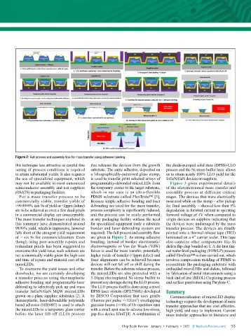
Figure 2: Full process and assembly flow for mass transfer using adhesive bonding.
        this technique less attractive as careful fine   that releases the devices from the growth   the diode-pumped solid state (DPSS)-LLO
        tuning of process conditions is required   substrate. The same adhesive, deposited on   process and the Ni stress buffer layer allows
        to attain substantial yields. It also requires   a lithographically-patterned glass stamp,   us to attain nearly 100% LLO yield for the
        the use of specialized equipment, which   is used to transfer print selected arrays of   InGaN/GaN devices on sapphire.
        may not be available in most outsourced   programmably-debonded microLEDs from   Figure 3 gives experimental details
        semiconductor assembly and test suppliers   the temporary carrier to the target substrate,   of the aforementioned mass transfer and
        (OSATS) or packaging facilities.   which in our case is an ultra-flexible   assembly process at different critical
          For a mass transfer process to be   PDMS substrate called FlexTrate™ [3].   stages. The devices that were electrically
        commercially viable, transfer yields of   Because simple adhesive bonding and laser   measured while on the stamp – after pickup
        >99.9999% (six 9s of yield or <1ppm failure)   debonding are used for the mass transfer,   for final assembly – showed less than 5%
        are to be achieved as even a few dead pixels   process complexity is significantly reduced,   degradation in forward current at operating
        in a commercial display are unacceptable.   and the process can be easily performed   forward voltage of 4V when compared to
        The mass transfer techniques explored in   at any packaging facility without the need   virgin devices on sapphire indicating that
        this summary have demonstrated around   for specialized equipment (only a substrate   the devices were undamaged by the mass
        99.99% yield, which is impressive, however   bonder and laser debonding system are   transfer process. The devices are finally
        falls short of the stringent yield requirement   required). The full process and assembly flow   printed onto a thermal release tape (TRT)
        of > six 9s for commercialization. Even   are given in Figure 2. As strong adhesive   laminated on a 4” carrier wafer. This tape
        though using post-assembly repairs and   bonding, instead of weaker electrostatic/  also contains other components like Si
        redundant pixels has been suggested to   electromagnetic or Van der Waals (VdW)   dielets flip-chip bonded on it. A die-first fan-
        overcome this yield issue, such solutions are   forces is used for mass transfer, potentially   out wafer-level packaging (FOWLP) process
        not economically viable given the high cost   higher yields of transfer (<1ppm defect) and   called FlexTrate™ is then carried out, which
        and time of repairs and material cost of the   finer alignments can be achieved because   involves compression molding of PDMS to
        microLEDs.                         devices will not fall off or shift during the   reconstitute the packaging substrate with
          To overcome the yield issues and other   transfer. Before the substrate release process,   embedded microLEDs and dielets, followed
        drawbacks, we are currently developing   the microLEDs are also protected with a   by fabrication of metal interconnects using a
        a transfer process using thermoplastic   5-10µm electroplated Ni stress buffer to   back end of line (BEOL) Cu plating process
        adhesive bonding and programmable-laser   prevent any damage during the LLO process.   and surface passivation using Parylene-C.
        debonding to selectively pick up and mass   The LLO process itself is done using a novel
        transfer InGaN/GaN MQW microLEDs   DPSS laser system (DFL7560L) developed   Summary
        grown on c-plane sapphire substrates [2]. A   by DISCO Corporation that uses gentle   Commercialization of microLED display
        thermoplastic, laser-debondable polyimide   (fluence per pulse <<1J/cm ) overlapping   technology requires the development of mass
                                                                 2
        based adhesive (HD3007) is used to attach   gaussian beams (>>10s of Hz repetition rate)   transfer approaches that are cost effective,
        the microLEDs to a temporary glass carrier   with a small spot size to achieve low-stress,   high yield, and easy to implement. Current
        before the laser lift-off (LLO) process   gap-free device liftoff [4]. A combination of   mass transfer approaches in literature and

                                                                                                             55
                                                          Chip Scale Review   January  •  February  •  2021   [ChipScaleReview.com]  55

