Page 52 - ChipScale_Jan-Feb_2021-digital
P. 52
High-throughput flexible direct imaging for


        packaging/MEMS fabrication


        By Shota Majima, David Hyde  [SCREEN Semiconductor Solutions Co., Ltd.]
        T          he r e a r e a nu mb e r of   production and the complexity in resulting   the GLV™ functions as a programmable


                   direct imaging systems for
                                           has become a financial burden and a
                                                                              modulation and switching of laser light
                   advanced packaging and   processes. The combination of these factors   diffraction grating, enabling attenuation,
        microelectromechanical systems (MEMS)   design constraint to manufacturers. In fact,   with unparalleled resolution, speed, and
        applications. Several are discussed in the   MEMS manufacturing and some advanced   precision. Using this new technology, we
        sections below, and this article will propose   packaging techniques, like heterogeneous or   have developed a flexible direct imaging
        using direct imaging for the die-first fan-  chiplet integration, are now looking toward   system for advanced packaging and MEMS
        out packaging of heterogeneous devices   maskless systems to resolve these issues.   industries with support for resolutions down
        that use high-density organic interconnects.   Especially in die-first fan-out packaging   to 2/2µm. When configured with multiple
        This last application will be key for future   technology, the flexible compensation   exposure heads, this system can process
        high-performance computing (HPC).  exposure of a maskless system is necessary   a wide range of substrate types, from
                                           to achieve production level throughput   200mm/300mm wafers up to 600mm square
        Mask-less direct imaging           with the high-overlay accuracy needed   panels. The ability to control the reflected
        lithography                        to maintain yield. The stepper/aligner   light level by changing the electrical bias
          The most common patterning method   approach of mask-based lithography enjoys   at each ribbon allows the use of multiple
        of semiconductor microfabrication is to   high overlay accuracy, but often does so at   exposure dose levels (grayscale exposure)
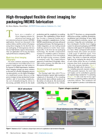
        project a mask pattern onto the surface to   the expense of throughput.  in the same exposure operation. Figure 1
        be exposed. In R&D departments, maskless                              illustrates the light valve’s structure (Figure
        direct imaging systems are more common   Direct imaging with spatial light   1a), including grayscale exposure samples.
        as the need for a flexible lithography process   modulator            With grayscale exposure, the resist side
        has taken priority over the higher throughput   The Grating Light Valve (GLV™) is a   wall angles can be controlled to generate
        of a mask-based system. However, as the   high-performance spatial light modulator   the tapered shape needed for Cu sputtering
        pattern designs in mass production become   composed of thousands of free-standing   (Figure 1b) and avoid the reverse taper
        smaller, and of increasing complexity,   silicon-nitride micro-ribbons anchored on   that leads to sputtering defects and plating
        the cost of manufacturing the device is   the surface of a silicon die. By electronically   continuity failures. This technique can
        increasing, partially driven by the mask   controlling the deflection of the ribbons,   also be applied to produce dual-damascene


        Figure 1: Illustration of GLV™ a) structure, b) taper shape control, and c) application to dual-damascene lithography.

        50   Chip Scale Review   January  •  February  •  2021   [ChipScaleReview.com]
        50

