Page 48 - ChipScale_Jan-Feb_2021-digital
P. 48
backgrinding (BG), chemical vapor
                                                                              deposition (CVD), or other chemical
                                                                              processes. By hardening the adhesive
                                                                              layer before loading into several
                                                                              p r o c e s s e s , t he d eg r a d a t io n a nd
                                                                              softening of the adhesive layer during
                                                                              these processes can be prevented.
                                                                              To distinguish this UV irradiation at
                                                                              405nm for polymerization of the resin
                                                                              before chemical or thermal processing
                                                                              from the use of UV irradiation at
                                                                              254n m  for  N 2  gas  generation,  we
                                                                              refer  to  the  405  nm-wavelength  UV
                                                                              irradiation as “pre-UV.” By using pre-
                                                                              UV irradiation, the adhesive got rigid
                                                                              and the adhesion strength gets lower.
                                                                              This crosslinking of the adhesive resin
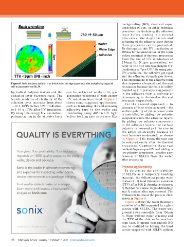
        Figure 4: Wafer thickness variation in an 8-inch wafer and edge appearance after backgrinding supported   also improves chemical and thermal
        with a glass carrier and SELFA.                                       resistances because the resin is stiffly
                                                                              bonded and it prevents components
        by radical polymerization and the   ca n be a ch ieve d w it hout N 2  ga s   in the adhesive from dissolving or
        adhesion layer becomes rigid. The   generation occurring if high-energy   decomposing in chemical or thermal
        tensile  modulus  of  elasticity  of  the   UV radiation were used.  Figure 3   processes, respectively.
        adhesion layer increases from about   shows some suggested applications,   For t he s e c ond a p p r o a ch – t o
                 4
        1~10 x 10 Pa before UV irradiation,   such as laminating the self-releasing   decrease affinity to the adherend – the
                   6
        to 1~10 x 10 Pa after UV irradiation.   a d h e sive t a p e  t o  t h e wa fe r a n d   surface polarity of the adhesive resin
        By using low-energy UV irradiation,   irradiating using  405nm  UV light   is controlled by adding low polarity
        polymerization in the adhesive layer   before loading into processes like   components into the adhesive layers.
                                                                              By adding low polarity components
                                                                              to the adhesive layers, the surface
                                                                              polarity is lowered and the rise in
                                                                              the adhesion strength because of
                                                                              heat becomes moderated, as shown
                                                                              in Figure 3. This means the tape can
                                                                              be removed easily after the thermal
                                                                              processes. Combi ni ng these t wo
                                                                              methodologies—pre-UV and adding a
                                                                              low polarity component—enables easy
                                                                              removal of SELFA from the wafer
                                                                              after processing.

                                                                              Process applicability
                                                                                To deter mine the applicabilit y
                                                                              of  SELFA  as  a  temporary  bonding
                                                                              material, the following points were
                                                                              evaluated: 1) total thickness variation
                                                                              (TTV) after BG; 2) chemical resistance;
                                                                              3) thermal resistance; 4) gas debonding;
                                                                              and 5) residue after tape removal. The
                                                                              evaluation followed the process flow
                                                                              shown in Figure 3.
                                                                                Figure 4 shows the wafer thickness
                                                                              variation after BG supported by a glass
                                                                              carrier with SELFA. The wafer was
                                                                              ground down smoothly from 750µm
                                                                              to 50µm without wafer cracking and
                                                                              the TTV of the thin wafer was less
                                                                              than 3µm. It means that smooth BG
                                                                              can be realized by having the hard
                                                                              carrier supported with SELFA without


        46
        46   Chip Scale Review   January  •  February  •  2021   [ChipScaleReview.com]

