Page 45 - ChipScale_Jan-Feb_2021-digital
P. 45
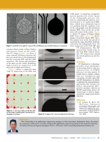
UBM panel. A repeating rectangular
                                                                              pattern matches the reticle layout
                                                                              of t he l it hog r aphy process. T he
                                                                              defects comprising the pattern were
                                                                              determined to be undersized RDL
                                                                              lines, which were ultimately traced
                                                                              to a problem with the condenser lens
                                                                              of the lithography tool that produced
                                                                              thinner RDL lines on the die at the
                                                                              lower left corner of the reticle. Figure
                                                                              9a shows CF images of thinner (8µm)
                                                                              R DL lines and  Figure 9b shows
                                                                              images of normal (14µm) RDL lines.
                                                                              Five panels were in the lot and all of
                                                                              them had the same thin RDL problems
                                                                              caused by the lithography tool. All
        Figure 7: a) (left) BF and b) (right) CF images of RDL and UBM pads captured with 4X objective (1.75µm/pixel)  were inspected with both BF and
                                                                                      CF  illu m i nat ion.  T he  BF
        nuisance defect counts without finding                                        inspections found none of
        real process issues on the wafer.                                             the thin RDL defects while
        The CF image (Figure 7b) shows a                                              the CF inspections fou nd
        clear contrast difference between the                                         the reticle pattern on all five
        previous metal layer in the background                                        panels.
        and the overlying RDL and the UBM
        structures. The texture and graininess                                        Summary
        of the metal are not visible, permitting                                       CF illumination technology
        high-sensitivit y  i nspection  with                                          provides clear advantages
        detection of single-pixel defects.                                            in detecting defects that are
          Figure 8 shows a composite map                                              ch a r a c t e r i s t ic  of  FOPL P
        from CF inspection of the RDL and                                             processes on large panels. It
                                                                                      readily detects organic residues
                                                                                      t h a t a r e t r a n s p a r e nt a n d
                                                                                      essentially invisible under BF
                                                                                      and DF illumination. Its ability
                                                                                      to eliminate the metal graininess
                                                                                      and texture that obscure real
                                                                                      defects and generate false-
                                                                                      positive nuisance defects in
                                                                                      BF/DF inspections allows CF
                                                                                      technology to deliver high-
                                                                                      sensitivity single-pixel defect
                                                                                      detection.

                                                                                      Reference
                                                                                      1.  G. Si ng h , K . Best , R .
                                                                                         M c Cl e a r y “A d v a n c e d
                                                                                         packaging lithography and
                                                                                         inspection solution for next-
                                                                                         generation FOWLP-FOPLP
        Figure 8: CF panel map of defects on the RDL/UBM
        sample reveals a repeating pattern that matches the                              processing,” IEEE Xplore,
        lithography reticle layout.        Figure 9: CF images of thin (top) and normal (bottom) RDL lines.  Oct. 2016.


                       Biography
                         Woo Young Han is an applications engineering manager at Onto Innovation, Richardson, Texas. He joined
                       the company in 2000 and is currently managing the applications engineering group for the inspection business.
                       He holds an Electrical Engineering degree from U. of Toronto. Email wooyoung.han@ontoinnovation.com


                                                                                                             43
                                                          Chip Scale Review   January  •  February  •  2021   [ChipScaleReview.com]  43

