Page 41 - ChipScale_Jan-Feb_2021-digital
P. 41
Revealing invisible defects on large 600mm panels


        By Woo Young Han  [Onto Innovation]
        I     n their continuing drive to pack   small size ultimately limits the space   Challenges of FOPLP


              more computing power and speed
                                                                                As with most things electronic, there
                                             Fan-out wafer-level processing. Fan-
              into less space, semiconductor   available for I/O connections.  is ever-present pressure to reduce feature
        manufacturers are using advanced   out wafer-level processing (FOWLP) offers   dimensions and spacing and to increase
        packaging (AP) processes to integrate   increased I/O capability. Separated chips   substrate size. Panel sizes have already
        multiple die of different types within a single   are embedded in a round substrate with   grown as large as 730mm X 920mm
        package and to increase input/output (I/O)   space added between the chips. Overlying   and larger sizes are possible. The large
        connectivity for large, complex chips. The   redistribution layers (RDL) route signals   number of expensive known-good-die
        use of front-end-like processes to create ever   from contacts on the top surface of the chip   contained on a panel makes process failures
        smaller features on ever larger substrates is   to contacts on the top surface of the larger   especially costly. Panels require handlers
        increasing the need for process control and   substrate extending beyond the area of the   designed to accommodate not only their
        inspection in AP processes. Novel materials   chip itself. The round, wafer-like form factor   rectangular shape, but also their increased
        like organic polymer dielectrics pose   of the reconstituted FOWLP substrates   size and weight. Challenges associated with
        special challenges to conventional front-end   permits the use of process equipment and   accurately positioning die, measuring shifts
        optical technologies. Our new illumination   handlers designed for wafer processing with   that unavoidably occur during the process
        technology, Clearfind®, specifically   minimal modification. But it also limits   [1], and maintaining the flatness of the
        addresses these issues to provide high-  the size of the substrate (and therefore the   repositioned die and the overall panel are
        sensitivity defect detection.      number of die that it can contain), and it   also nontrivial.
                                           wastes space near the curved edges of the   This article focuses on inspection
        Packaging evolution                substrate where rectangular die/packages do   challenges for FOPLP processes. RDL line
          Packaging processes have evolved from   not fit efficiently.        widths are now typically in the few tens of
        relatively simple, inexpensive technologies to   Fan-out panel-level processing. Fan-out   micrometers range, but line widths down
        costly, complex processes that have adopted   panel-level processing (FOPLP) is similar to   to 1µm-2µm are on many roadmaps. This
        and adapted process technologies developed   FOWLP except the panel substrates are not   implies the need for inspection sensitivity to
        for wafer fabrication. Some of these processes   limited to wafer-like form factors. They can   defects as small as 0.5µm. Although defects
        are discussed in the sections below.  be rectangular, to increase spatial efficiency,   of this size are well within the detection
          Wire bonding. Traditionally, packaging   and larger, to process more die per panel at   range of optical inspection technologies, the
        uses thin wires bonded between I/O pads at   lower cost per die.      materials used in FOPLP processes raise
        the edge of the chip and a wire frame that
        includes pins for connection to a printed
        circuit board. The chip and frame are
        encapsulated for protection from the external
        environment, resulting in a final package that
        is much larger than the chip.
          Flip chip. Chip-scale processes, like flip
        chip, form contact pads on the top surface
        of the die, which, when the separated die
        are flipped over, mate with solder balls on
        a connecting package substrate. Flip-chip
        packages allow many more I/O connections
        because the entire surface of the chip, not
        just the edges, can be used for contacts.
        The resulting package is smaller than wire
        bonding, but usually larger than the chip.
          Wafer-level processing. Wafer-level
        processing (WLP) uses front-end-like
        processes to form packaging structures
        on chips while they are still part of the
        wafer on which they are fabricated. WLP
        has the benefit of creating small packages
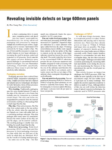
        – the same size as the chip – but that   Figure 1: Simplified illustrations of the differences between traditional white light BF and DF illumination and
                                           CF technology.

                                                                                                             39
                                                          Chip Scale Review   January  •  February  •  2021   [ChipScaleReview.com]  39

