Page 36 - ChipScale_Jan-Feb_2021-digital
P. 36
Extreme Si thinning and nano-TSVs to advance 3D


        heterogeneous integration


        By Dave Thomas  [SPTS Technologies]  Anne Jourdain  [imec]
        I     t is anticipated that most of


              the 3D system on chip (SoC)
              integration schemes for the
        future  will  require  wafer-to-wafer
        (W2W) bonding, which directly joins
        the back-end-of-line (BEOL) layers of
        two wafers, in combination with via-last
        through-silicon via (TSV) connections.
        This article presents a new approach
        that combines extreme thinning of
        silicon to a final thickness of 500nm,
        together with subsequent etching of
        nano-scale TSVs at sub-500nm pitch.
        This allows  for  very high-density
        electrical connections between the back
        side and front side of a device wafer
        as part of the back-side power delivery
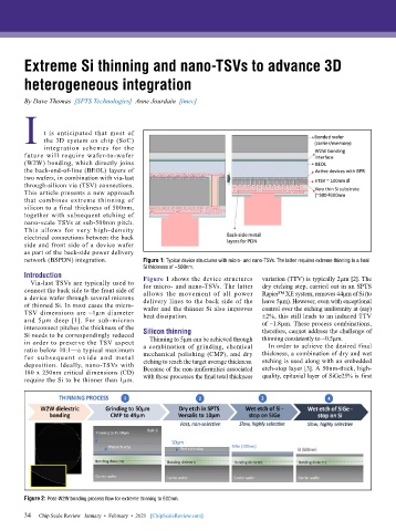
        network (BSPDN) integration.       Figure 1: Typical device structures with micro- and nano-TSVs. The latter requires extreme thinning to a final
                                           Si thickness of ~500nm.
        Introduction                       Figure 1 shows the device structures   variation (TTV) is typically 2µm [2]. The
          Via-last TSVs are typically used to   for micro- and nano-TSVs. The latter   dry etching step, carried out in an SPTS
        connect the back side to the front side of   allows the movement of all power   Rapier™ XE system, removes 44µm of Si (to
        a device wafer through several microns   delivery lines to the back side of the   leave 5µm). However, even with exceptional
        of thinned Si. In most cases the micro-  wafer and the thinner Si also improves   control over the etching uniformity at (say)
        TSV dimensions are ~1µm diameter   heat dissipation.                  ±2%, this still leads to an induced TTV
        and 5µm deep [1]. For sub-micron                                      of ~1.8µm. These process combinations,
        interconnect pitches the thickness of the                             therefore, cannot address the challenge of
        Si needs to be correspondingly reduced   Silicon thinning             thinning consistently to ~0.5µm.
        in order to preserve the TSV aspect   Thinning to 5µm can be achieved through   In order to achieve the desired final
        ratio below 10:1—a typical maximum   a combination of grinding, chemical   thickness, a combination of dry and wet
        for subse que nt ox ide a nd met al   mechanical polishing (CMP), and dry   etching is used along with an embedded
        deposition. Ideally, nano-TSVs with   etching to reach the target average thickness.    etch-stop layer [3]. A 50nm-thick, high-
        180 x 250nm critical dimensions (CD)   Because of the non-uniformities associated   quality, epitaxial layer of SiGe25% is first
        require the Si to be thinner than 1µm.   with these processes the final total thickness


        Figure 2: Post-W2W bonding process flow for extreme thinning to 500nm.

        34   Chip Scale Review   January  •  February  •  2021   [ChipScaleReview.com]
        34

