Page 38 - ChipScale_Jan-Feb_2021-digital
P. 38
be achieved between the front side and
                                                                              back side of an extremely thin device
                                                                              wafer. The electrical characterization
                                                                              consisted of single measurements of
                                                                              Kelvin resistance (for a single TSV)
                                                                              and lengthy daisy chains connecting
                                                                              f ront-side M1 to backside BSM1
                                                                              through multiple TSVs. The study also
                                                                              included the impact of overlay between
                                                                              the TSVs and M1. The detailed overlay
                                                                              data is beyond the scope of this article
                                                                              but, simply put, the Kelvin resistance
                                                                              is minimized when there is alignment
                                                                              between the TSV and M1, but also
                                                                              when the TSV etches beyond the M1
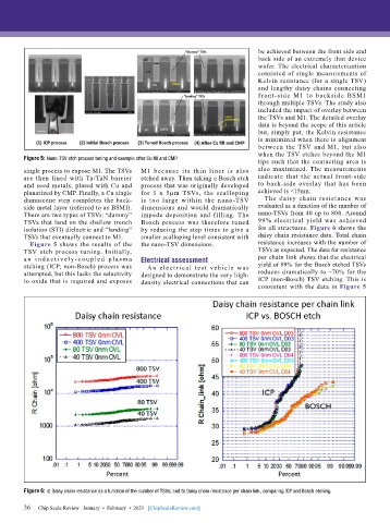
        Figure 5: Nano-TSV etch process tuning and example after Cu fill and CMP.  tips such that the contacting area is
        single process to expose M1. The TSVs   M1 because its thin liner is also   also maximized. The measurements
        are then lined with Ta/TaN barrier   etched away. Then taking a Bosch etch   indicate that the actual front-side
        and seed metals, plated with Cu and   process that was originally developed   to back-side overlay that has been
        planarized by CMP. Finally, a Cu single   for 1 x 5µm TSVs, the scalloping   achieved is <15nm.
        damascene step completes the back-  is too large within the nano-TSV    The daisy chain resistance was
        side metal layer (referred to as BSM1).   dimensions  and  would  dramatically   evaluated as a function of the number of
        There are two types of TSVs: “dummy”   impede deposition and filling. The   nano-TSVs from 40 up to 800. Around
        TSVs that land on the shallow trench   Bosch process was therefore tuned   99% electrical  yield was  achieved
        isolation (STI) dielectric and “landing”   by reducing the step times to give a   for all structures. Figure 6 shows the
        TSVs that eventually connect to M1.  smaller scalloping level consistent with   daisy chain resistance data. Total chain
          Figure 5 shows the  results of  the   the nano-TSV dimensions.      resistance increases with the number of
        TSV etch process tuning. Initially,                                   TSVs as expected. The data for resistance
        a n  i n d u c t i ve l y- c o u pl e d  pl a s m a   Electrical assessment  per chain link shows that the electrical
        etching (ICP; non-Bosch) process was   A n elect r ical test veh icle was   yield of 99% for the Bosch etched TSVs
        attempted, but this lacks the selectivity   designed to demonstrate the very high-  reduces dramatically to ~70% for the
        to oxide that is required and exposes   density electrical connections that can   ICP (non-Bosch) TSV etching. This is
                                                                              consistent with the data in Figure 5


        Figure 6: a) Daisy chain resistance as a function of the number of TSVs; and b) Daisy chain resistance per chain link, comparing ICP and Bosch etching.

        36   Chip Scale Review   January  •  February  •  2021   [ChipScaleReview.com]
        36

