Page 34 - ChipScale_Jan-Feb_2021-digital
P. 34

in delivering more data functionalities,
                                                                              thereby paving the way into 5G adoption.
                                                                              Pent-up demand is expected to return in
                                                                              2021 as more technology-related business
                                                                              leaders are increasingly optimistic that
                                                                              businesses and consumers will return
                                                                              to a new normal. FOPLP is projected to
                                                                              gain 13% in volume from 5% in 2019, to
                                                                              18% in 2025. At a 15% compound annual
                                                                              growth rate (CAGR), fan-out packaging is
                                                                              expected to be valued at $3.05B by 2025,
                                                                              up from $1.25B in 2019 [2,5].
                                                                                Some of the challenges encountered on
                                                                              600mm x 600mm FOPLP were discussed.
                                                                              We reviewed the impact of die shift in the
                                                                              x, y, and Ɵ directions in the chip attach
                                                                              process, and the use of laser-directed
                                                                              imaging to eliminate routing issues caused
                                                                              by die shift for RDL. We also reviewed
                                                                              CSAM metrology used for detecting mold
                                                                              defects on panel and die level process
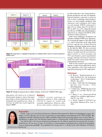
        Figure 11: 9 segments vs. 4 segments for chip attach on a 600mm x 600mm panel for 6-sided die protection.   optimizations to meet warpage and
        SOURCE: DECA                                                          TTV specifications, panel segmentation
                                                                              strategy, and keep out zones to maximize
                                                                              usable area and to ensure panel robustness
                                                                              at downstream processes.
                                                                                FOPLP will continue to gain traction and
                                                                              appeals to high-volume applications where
                                                                              a key application will be the enabling of
                                                                              large die partitioning for HPC applications.
                                                                              References
                                                                                1.  B. Rogers, “Implementation of a
                                                                                  fully-molded fan-out packaging
                                                                                  technology,” Deca Technologies,
                                                                                  IWLPC, Nov. 2013.
                                                                                2.  F. Shoo, “2020 Fan-Out Packaging
                                                                                  M a r k e t  a n d T r e n d s ,”  Yo l e
                                                                                  Développement.
                                                                                3.  J. Aman Lim, “eWLB fan-out as one
                                                                                  solution for 2.5D SiP,” IWLPC, Oct.
        Figure 12: Example of a keep-out zone on a 300mm round pan, for M-Series™. SOURCES: DECA, nepes.  2017.
        placement will need to be evaluated   Summary                           4.  F. Wang, F. An, “Advanced eWLB
        during panel design to ensure that panel   FOW L P r e ve nu e c o nt i nu e s t o   solutions for mmWave applications,”
        processing in downstream processes like   experience a decline in 2020, reflecting   IWLPC, Oct. 2018.
        backgrind and singulation are robust. A   COVID-19 impact for mobile and   5.  L. Wood, “Impact of COVID-19 on
        decrease in usable area would negatively   consumer applications. However, data-  the market,” Business Wire, Aug. 12,
        impact GDPP.                       driven end systems continue to grow    2020.


                       Biographies
                         Jacinta  Aman Lim is the Technical Director of Business Development for Wafer Level Packaging at nepes, San
                       Diego, CA USA. She has over 18 years of experience in semiconductor manufacturing, WLP, NPI and R&D. She
                       graduated with MSE (Material Science), MBA and BSEE (Electrical Engineering) degrees from Arizona State U.,
                       and Business Analytics from The Wharton School of the U. of Pennsylvania. Email Jacinta.AmanLim@nepes.co.kr
                         Yun Mook Park is the Process Engineering Manager for the 600mm panel-level processing line at nepes,
                       South Korea. He has over 18 years of experience in semiconductor manufacturing in wafer-level packaging,
                       process engineering and R&D.  He graduated from Young Nam U. in South Korea with a Bachelor of Science
          in Electronics Engineering.


        32
        32   Chip Scale Review   January  •  February  •  2021   [ChipScaleReview.com]
   29   30   31   32   33   34   35   36   37   38   39