Page 30 - ChipScale_Jan-Feb_2021-digital
P. 30

telecom and infrastructure is improving
                                                                              moderately in 2020 and expected to
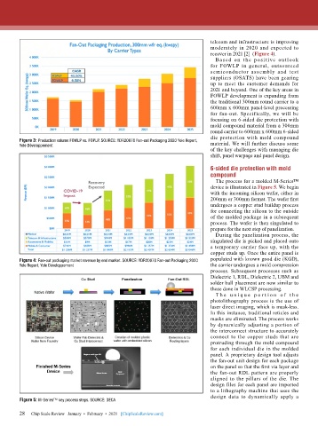
                                                                              recover in 2021 [2]  (Figure 4).
                                                                                Ba sed on t he posit ive outlook
                                                                              for  FOWLP  in  general,  outsourced
                                                                              semiconductor assembly and test
                                                                              suppliers (OSATS) have been gearing
                                                                              up to meet the customer demands for
                                                                              2021 and beyond. One of the key areas in
                                                                              FOWLP development is expanding from
                                                                              the traditional 300mm round carrier to a
                                                                              600mm x 600mm panel-level processing
                                                                              for fan-out. Specifically, we will be
                                                                              focusing on 6-sided die protection with
                                                                              mold compound material from a 300mm
                                                                              round carrier to 600mm x 600mm 6-sided
                                                                              die protection with  mold  compound
        Figure 3: Production volume FOWLP vs. FOPLP. SOURCE: YDR20078 Fan-out Packaging 2020 Yole Report,
        Yole Développement                                                    material. We will further discuss some
                                                                              of the key challenges with managing die
                                                                              shift, panel warpage and panel design.

                                                                              6-sided die protection with mold
                                                                              compound
                                                                                The process for a molded M-Series™
                                                                              device is illustrated in Figure 5. We begin
                                                                              with the incoming silicon wafer, either in
                                                                              200mm or 300mm format. The wafer first
                                                                              undergoes a copper stud buildup process
                                                                              for connecting the silicon to the outside
                                                                              of the molded package in a subsequent
                                                                              process. The wafer is then singulated to
                                                                              prepare for the next step of panelization.
                                                                                During the panelization process, the
                                                                              singulated die is picked and placed onto
                                                                              a temporary carrier face up, with the
                                                                              copper studs up. Once the entire panel is
        Figure 4: Fan-out packaging market revenue by end market. SOURCE: YDR20078 Fan-out Packaging 2020   populated with known good die (KGD),
        Yole Report, Yole Développement                                       the carrier undergoes a mold compression
                                                                              process. Subsequent processes such as
                                                                              Dielectric 1, RDL, Dielectric 2, UBM and
                                                                              solder ball placement are now similar to
                                                                              those done in WLCSP processing.
                                                                                T h e u n i q u e p o r t i o n o f t h e
                                                                              photolithography process is the use of
                                                                              laser direct imaging, which is mask-less.
                                                                              In this instance, traditional reticles and
                                                                              masks are eliminated. The process works
                                                                              by dynamically adjusting a portion of
                                                                              the interconnect structure to accurately
                                                                              connect to the copper studs that are
                                                                              protruding through the mold compound
                                                                              for each individual die in the molded
                                                                              panel. A proprietary design tool adjusts
                                                                              the fan-out unit design for each package
                                                                              on the panel so that the first via layer and
                                                                              the fan-out RDL pattern are properly
                                                                              aligned to the pillars of the die. The
                                                                              design files for each panel are imported
                                                                              to a lithography machine that uses the
                                                                              design data to dynamically apply a
        Figure 5: M-Series™ key process steps. SOURCE: DECA

        28
        28   Chip Scale Review   January  •  February  •  2021   [ChipScaleReview.com]
   25   26   27   28   29   30   31   32   33   34   35