Page 27 - ChipScale_Jan-Feb_2021-digital
P. 27
600mm wafer-level fan-out on panel-level processing


        with 6-sided die protection


        By Jacinta Aman Lim, YunMook Park, Byung Cheol Kim, Edil Devera [nepes]
        C         urrently, a 300mm carrier   This paper will present a case study   6.25mm fan-out package, was tested with


                  wafer for fan-out wafer-
                  level packaging (FOWLP)   of utilizing 600mm x 600mm panel   board-level temperature cycling (TC) on
                                                                              a 1mm board, with SAC405. The bump
                                           size to process a single die with 6-sided
        is the mainstream format used for power   die protection. Considerations for   pitch was at 500µm with no under bump
        management integrated circuits (PMICs),   repassivation, redistribution layer and   metallization (UBM). There were no TC
        radio frequency (RF) and other single-  solder ball placement will be discussed.   failures up to 1000 cycles. The plot in
        die applications. As the volume of these   Challenges pertaining to large panel   Figure 1 shows >200% improvement for
        devices continues to rise, the need for   processing through the repassivation and   TC over WLCSP [1].
        migration to panel sizes larger than 300mm   redistribution layer will be presented;
        becomes a necessity for cost reduction and   additionally, panel-level inspection   Fan-out packaging drivers
        capacity.                          considerations post mold cure, reliability   As can be seen from Figure 2, some
          The fastest adoption of fan-out   considerations, and the future of 600mm x   of the major market drivers are RF, audio
        technology is now in 5G, automotive and   600mm panel-level processing for 6-sided   codec, PMIC, radar, 5G and high-speed
        healthcare. Traditional applications such   die protection will be summarized.  computing [2].
        as audio codecs, PMICs, micro-controller                                5G adoption is central to large data
        units (MCU) and RF continue to use   Introduction to wafer-level      transfers to enable a new user experience,
        FOWLP as an alternative to wafer-level   packaging                    and enabling better cloud-based business
        chip-scale packaging (WLCSP) due to its   There are several types of wafer-  management as well as increasing our
        5-sided or 6-sided die protection. As fan-  level packaging (WLP) in the industry.   level of interaction with one another. In
        out packaging becomes mainstream and   The mainstream is WLCSP, or fan-in,   comparison to flip-chip ball grid array
        in order to get broader adoption of it, the   followed by variations of FOWLP. In the   (FCBGA) packages, the interconnect
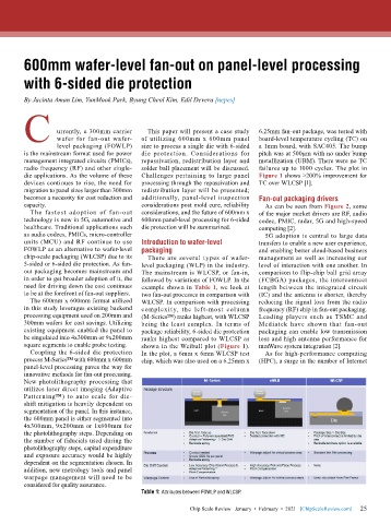
        need for driving down the cost continues   example shown in Table 1, we look at   length between the integrated circuit
        to be at the forefront of fan-out suppliers.   two fan-out processes in comparison with   (IC) and the antenna is shorter, thereby
          The 600mm x 600mm format utilized   WLCSP. In comparison with processing   reducing the signal loss from the radio
        in this study leverages existing backend   complexity, the left-most column   frequency (RF) chip in fan-out packaging.
        processing equipment used on 200mm and   (M-Series™) ranks highest, with WLCSP   Leading players such as TSMC and
        300mm wafers for cost savings. Utilizing   being the least complex. In terms of   Mediatek have shown that fan-out
        existing equipment enabled the panel to   package reliability, 6-sided die protection   packaging can enable low transmission
        be singulated into 4x300mm or 9x200mm   ranks highest compared to WLCSP as   loss and high antenna performance for
        square segments to enable probe testing.   shown in the Weibull plot (Figure 1).   mmWave system integration [2].
          Coupling the 6-sided die protection   In the plot, a 6mm x 6mm WLCSP test   As for high-performance computing
        process M-Series™ with 600mm x 600mm   chip, which was also used on a 6.25mm x   (HPC), a surge in the number of Internet
        panel-level processing paves the way for
        innovative methods for fan-out processing.
        New photolithography processing that
        utilizes laser direct imaging (Adaptive
        Patterning™) to auto scale for die-
        shift mitigation is heavily dependent on
        segmentation of the panel. In this instance,
        the 600mm panel is either segmented into
        4x300mm, 9x200mm or 1x600mm for
        the photolithography steps. Depending on
        the number of fiducials used during the
        photolithography steps, capital expenditure
        and exposure accuracy would be highly
        dependent on the segmentation chosen. In
        addition, new metrology tools and panel
        warpage management will need to be
        considered for quality assurance.
                                           Table 1: Attributes between FOWLP and WLCSP.

                                                                                                             25
                                                          Chip Scale Review   January  •  February  •  2021   [ChipScaleReview.com]  25

