Page 22 - ChipScale_Jan-Feb_2021-digital
P. 22
complete daisy chain that can be tested   respectively to complete each S-MCM.   excess of 50mA at 4.2K. The large number
        for continuity and total resistance.   Additionally, because of minimum   of microbumps per chip, compact bump
        These  devices  are  surrogates  for  a   spacing and edge keep-out regions for   geometry, high critical current of niobium,
        superconducting wafer-scale MCM and   dicing and in-line metrology, 2-chip (   and high current-carrying capacity of
        the associated superconducting chips to   20mm x 20mm) S-MCMs can have a   the microbumps enable this process
        be connected. The current microbump   significantly higher active circuit area   to be suitable for building VLSI flip-
        fabrication process uses a single I-line   compared to a 16-chip S-MCM for a   chip structures and developing complex
        liftoff process on the superconducting   given lithography process.   superconducting computing systems.
        MCM. An interconnect layer (1000nm   As a case study of larger area flip-
        Nb, 20nm Ti, 50nm Pt, 150nm Au,    chip interconnections, a 25mm x    Stitched S-MCM
        20 0 0 n m I n) a n d a n u n d e r b u m p   25mm S-MCM with niobium-indium   I n t h i s s e c t ion , we d e t a i l t he
        metalization (UBM) layer (1000nm   microbumps and a 20mm x 20mm       fabrication processes for reticle stitching.
        Nb, 20nm Ti, 50nm Pt, 150nm Au)    superconducting chip were bonded   The previously described single reticle-
        are evaporated onto the S-MCM, and   together to fabricate a daisy chain   based S-MCM fabrication process
        superconducting chips, respectively.   structure. By alternating daisy chains in   was modified to create a larger area
        The I-line photo process is important   the lay-up prior to bonding, the Nb-In   stitched S-MCM. Figure 2 represents
        for reducing wafer-scale photoresist   microbumps electrically connect the daisy   the stitching process where circuit lines
        defects, def ining bump diameter,   chains. The S-MCMs include a 20mm   of individual reticles are stitched at a
        and improved alignment to maintain   x 20mm flip-chip daisy chain structure   stitch boundary. Four I-line photomasks
        electrical properties and minimize   prepared with approximately 10,000 or   (A, B, C, D) were joined together to
        bump-bonding issues.               100,000 niobium-indium microbumps.   create a stitched field. Photomask A
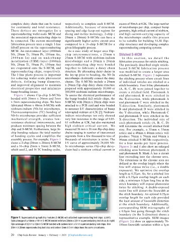
          Figure 1 shows flip-chip S-MCMs   To assess the electrical performance of   and photomask B were stitched in
        bonded with 20mm x 20mm and 5mm    the bump bonded full reticle chips, the   the X-direction, while photomask A
        x 5mm superconducting chips. We have   S-MCMs with 20mm x 20mm chips were   and photomask C were stitched in the
        fabricated 48mm x 48mm S-MCMs with   attached to a PCB card and wire bonded   Y-direction. Similarly, photomask
        niobium-indium (Nb-In) microbumps.   to measure I-V characteristics of bump   B and photomask D were stitched in
        Thermocompression (TC) bonding of   interrupted niobium at 4.2K [2]. Niobium-  the Y-direction, while Photomask C
        Nb-In microbumps provides sufficient   indium microbumps not only showed   and photomask D were stitched in the
        mechanical strength, creates low-  very low resistance in the range of 0.05-  X-direction. The individual size of
        resistance electrical interconnects, and   0.1 milliohm at 4.2K, but also maintained   each photomask reticle (A, B, C, D)
        produces minimum spacing between the   high niobium critical current.  We   will determine the overall stitched field
        chip and S-MCM. Furthermore, large Si-  measured 20 mm x 20 mm flip-chip daisy   size.  For  example,  a  35mm  x  35mm
        chip bonding reduces the total number   chains ranging in number of interconnect   reticle and a 48mm x 48mm reticle will
        of bonding cycles and simplifies the   segments from a few thousand to tens of   produce 70mm x 70mm and 96mm x
        assembly process. For example, Figure 1   thousands of microbumps in series. The   96mm stitched S-MCMs respectively,
        shows a 2-chip (20mm x 20mm) S-MCM   I-V curve of approximately 24,000 Nb-  for  a  four  masks  per  layer  process.
        and a 16-chip (5mm x 5mm) S-MCM,   In microbumps series flip-chip daisy-  Figures 2c and d also show an enlarged
        which used 2, and 16 TC bonding cycles,   chain had a niobium critical current in   stitching area between photomask A
                                                                              and photomask B. Mask A has a circuit
                                                                              line extending into the chrome area.
                                                                              The extensions in the chrome area are
                                                                              defined as the overlap length where the
                                                                              line will expose twice (i.e., a double
                                                                              exposure). We optimize the overlap
                                                                              length as 0.25μm. So, for a stitched line
                                                                              with a 0.25μm overlap length on each
                                                                              side, a minimum 0.5μm long line at the
                                                                              stitch boundary will expose photoresist
                                                                              twice for stitching. A double-exposed
                                                                              resist line will distort the linewidth at
                                                                              the stitch boundary. An optimal 0.25μm
                                                                              overlap length for each side provided
                                                                              the least amount of linewidth distortion
                                                                              at the stitch boundary. Additionally,
                                                                              corresponding SEM micrographs of
                                                                              a 0.8μm line going through the stitch
                                                                              boundary (in the X-direction) shows a
        Figure 1: Superconducting multichip modules (S-MCM) with attached superconducting test chips: a) (left)   representative example. SEM images
        Optical image of a 48mm x 48mm S-MCM bonded with two 20mm x 20mm superconducting test chips; b) (right)   (Figure 2e) show an approximately 70-
        Optical image of 32mm x 32mm S-MCM bonded with sixteen 5mm x 5mm superconducting test chips. One   110nm linewidth variation within a 1μm
        20mm X 20mm superconducting test chip and sixteen 5mm X 5mm chips have the same circuit area.

        20   Chip Scale Review   January  •  February  •  2021   [ChipScaleReview.com]
        20

