Page 18 - ChipScale_Jan-Feb_2021-digital
P. 18
spindle height to control for any
        variation identified.
          Studies were conducted to determine
        baseline system performance using the
        AMS, such that any spindle variation
        over  time  could  then  be  controlled
        (Figure 7). As can be seen from the
        results, AMS can resolve down to system
        accuracies of <3.2µm @ Cpk 1.33.
          Substrate and interconnect dimensions
        require placement capability over large
        substrates up to 600mm x 600mm
        at sub-10µm XY accuracy and sub-
        0.075º theta accuracy to achieve high
        yield. Placement rates of >16K have
        been demonstrated at this performance
        level—a key aspect to minimizing the
        cost of assembly.
          Additionally, as die thicknesses
        are reduced below 100µm, there is
        an increased potential for cracking,
        chipping or uncontrolled warpage when
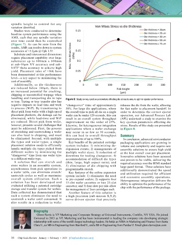
        handling and transporting die in tape   Figure 8: Study on key ejection parameters affecting die stress to ensure optimal ejector performance.
        or tray. Taping or tray transfer also has
        negative impacts on lead time and work   “changeover” time of approximately   releases the die from the wafer, allowing
        in process (WiP). By transitioning to   50%. For large die applications, where   for fast wafer to placement handoff. In
        direct pick from wafer with a high-speed   the overall time to pick all die on a single   order to determine the correct ejector
        placement platform, die damage can be   wafer can be under 120 seconds, this can   operation, our Advanced Process Lab
        eliminated, while lead-time and WiP   result in an overall system throughput   (APL) undertook a study to examine the
        are reduced. Direct pick from wafer,   improvement on the order of 25%.   key ejection parameters affecting die
        however, presents several challenges that   Likewise, for heterogeneous integration   stress. Results of this study are presented
        must be addressed. First, the process   applications where a wafer exchange   in Figure 8.
        of stretching and unstretching a wafer   may occur in as few as 30 seconds,
        can also lead to chipping, and must   this can lead to overall throughput   Summary
        be eliminated. Second, with multiple   improvements of up to 100%.      In conclusion, advanced semiconductor
        die types and wafer types, a single   Key benefits of the patented cartridge   packaging applications are growing in
        placement solution needs to efficiently   system  includes:  1)  minimizing  de-  volume and complexity and require new
        handle multiple die types picked from   expansion events; 2) managements of   assembly solutions to ensure high yield
        different wafers by minimizing the   multiple wafer sizes; 3) reduction of   at the best overall cost per placement.
        “changeover” time from one wafer type   downtime for tooling changeover; 4)   Innovative solutions have been assessed
        to a different wafer type.         accommodation of difficult die types   and proven to be viable, delivering the
          A solution that can stretch and   (thin,  large,  high  aspect  ratio);  and   required accuracy over the SEMI standard
        store wafers in an assembly system,   5) elimination of die chipping with   large panel format.  These solutions have
        asynchronous from pick operations in   programmable stretch.          additionally demonstrated the speed
        a wafer table, can eliminate stretch/  Key features of the online expansion   and utilization required for efficient
        unstretch cycles as well as maximize   system include: 1) eliminates the need   and economic assembly operations.
        overall system utilization. Such a   to pre-expand wafers; 2) supports four   Heterogeneous integration delivers the
        solution has been developed and    13-slot wafer cassettes or two 25-slot
        evaluated utilizing a patented cartridge   cassettes; and 3) four slots per side allow   ability to optimize the performance of the
        storage and transfer system for wafers.   for management of four cartridges each.  chip with the performance of the package.
        Data collected has demonstrated that   Another feature of this solution is
        such a system eliminates the need to   a high-precision (sub-micron X,Y,Z)
        unstretch a wafer until consumed. It   servo-driven ejector that precisely
        also results in a reduction in wafer


                       Biography
                         Glenn Farris is VP Marketing and Corporate Strategy at Universal Instruments, Conklin, NY USA. He joined
                       Universal in 2013 as VP, Marketing and has been instrumental in leading the company into developing strategic
                       relationship with some of the world’s largest technology leaders. He holds an MBA in Marketing and Finance from Santa
                       Clara U., an MS in Engineering from Stanford U., and a BS in Engineering from Purdue U. Email glenn.farris@uic.com


        16
        16   Chip Scale Review   January  •  February  •  2021   [ChipScaleReview.com]

