Page 15 - ChipScale_Jan-Feb_2021-digital
P. 15
Heterogeneous integration
          Moore’s law is still  providing a
        reduction in transistor size by a factor
        of two each year, but in the most
        advanced nodes we are no longer getting
        a corresponding reduction in cost. The
        combination of the need for performance
        advancement at lower cost is leading to
        new architectural paradigms. Printed
        ci rcuit boa rd assembly ( PCBA) -
        based systems need to shrink into
        microelectronic form factors to address
        the needs of edge computing. SoC
        semiconductor devices are disaggregating
        to optimize process nodes by function.
          The net result of the disaggregation
        noted above is a new approach to device
        packaging: heterogeneous integration.
        Rather than trying to cram functionality              ®
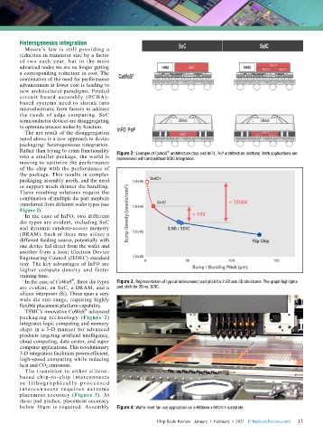
        into a smaller package, the world is   Figure 2: Example of CoWoS  architecture (top) and InFO_PoP architecture (bottom). Both applications are
                                           represented with and without SOIC integration.
        moving to optimize the performance
        of the chip with the performance of
        the package. This results in complex
        packaging assembly needs, and the need
        to support much thinner die handling.
        These resulting solutions require the
        combination of multiple die part numbers
        transferred from different wafer types (see
        Figure 2).
          In the case of InFO, two different
        die types are evident, including SoC
        and dynamic random-access memory
        (DRAM). Each of these may utilize a
        different feeding source, potentially with
        one device fed direct from the wafer and
        another from a Joint Electron Device
        Engineering Council (JEDEC) standard
        tray. The key advantages of InFO are
        higher compute density and faster
        training time.
                           ®
          In the case of CoWoS , three die types   Figure 3: Representation of typical interconnect pad pitch for 2.5D and 3D structures. The graph highlights
        are evident, an SoC, a DRAM, and a   pad pitch for 2D vs. SOIC.
        silicon interposer (Si). These span a very
        wide die size range, requiring highly
        flexible placement platform capability.
                                ®
          TSMC’s innovative CoWoS  advanced
        packaging technology (Figure 2)
        integrates logic computing and memory
        chips in a 3-D manner for advanced
        products targeting artificial intelligence,
        cloud computing, data center, and super
        computer applications. This revolutionary
        3-D integration facilitates power-efficient,
        high-speed computing while reducing
        heat and CO 2  emissions.
          The transition to either silicon-
        based chip-to-chip interconnects
        o r l i t ho g r a p h i c a l l y - p r o c e s s e d
        i nt e rc o n ne ct s re qu i r e s ex t r e me
        placement accuracy (Figure 3). At
        these pad pitches, placement accuracy
        below 10µm is required. Assembly   Figure 4: Wafer-level fan-out application on a 600mm x 600mm substrate.

                                                                                                             13
                                                          Chip Scale Review   January  •  February  •  2021   [ChipScaleReview.com]  13

