Page 23 - ChipScale_Jan-Feb_2021-digital
P. 23
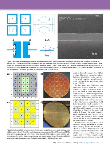
Figure 2: Illustration of the stitching process with I-line clear field photomasks. The blue color defined in the images is a chrome layer in the mask: a) (top left) Four
        individual (A, B, C, D) pre-stitched reticles and their orientation prior to stitching; b) (top right) A stitched reticle. Stitching of the four individual reticles produces a single
        stitched field. For example, four 35mm x 35mm individual reticles will produce a 70mm x 70mm-stitched field. The bottom images represent an enlarged stitch area: c)
        (bottom left) This image represents a circuit line within individual reticles prior to stitching, and d) (bottom right) represents a circuit line stitched in the stitched reticle. e)
        SEM micrographs of a 50 Ohms (0.8μm) line at the stitch boundary with a 0.25μm overlap.
                                                                              length at the stitch boundary for a 0.25μm
                                                                              overlap. Electrical simulation shows
                                                                              that these kind of linewidth variations
                                                                              at the stitch boundary are electrically
                                                                              small and have little impedance effect
                                                                              below 1THz [3].
                                                                                We have designed, fabricated, and
                                                                              tested two stitched S-MCMs. Figure
                                                                              3 shows examples of stitched S-MCM
                                                                              based on 35mm X 35mm and 48mm X
                                                                              48mm reticles. A stitched design includes
                                                                              a variety of impedance controlled lines,
                                                                              resonators, snake/combs, and via chains
                                                                              going back and forth between one reticle
                                                                              to the other and measured linewidth
                                                                              distortion at the stitch boundary. For
                                                                              example, a variety of snake/comb lines
                                                                              with linewidth/space ranging from
                                                                              0.8μm/1μm to 2μm/2μm that travel back
                                                                              and forth through the stitch boundary
                                                                              were evaluated and compared to
                                                                              reference structures that were located
                                                                              away from the stitch boundary and did
                                                                              not see the stitching process.
                                                                                Wafer-scale room-temperat u re
                                                                              electrical testing was used to evaluate
                                                                              reticle stitching. Each S-MCM wafer has
                                                                              a total of 384 test structures and each
        Figure 3: A stitched S-MCM wafer before dicing. Each design targeted a different reticle size for stitching: a) (top   structure consists of snake/combs with
        left) Schematic of a 35mm X 35mm I-line reticle stitching approach to create two 70mm X 70mm stitched S-MCMs;   LW/LS in the range of 0.8μm/1μm and
        b) (top right) A corresponding image of two 70mm x 70mm stitched S-MCMs on a 200mm wafer; c) (bottom left)   larger. Out of 384 test structures, 96
        Schematic of a 48mm x 48mm I-line reticle stitching approach to create a single 96mm x 96mm stitched S-MCM;   test structures are stitched. As desired,
        and d) (bottom right) Corresponding image of a 96mm x 96mm stitched S-MCM on a 200mm wafer.

                                                                                                             21
                                                          Chip Scale Review   January  •  February  •  2021   [ChipScaleReview.com]  21

