Page 24 - ChipScale_Jan-Feb_2021-digital
P. 24
achieve  a  50Ω  impedance  without
                                                                              changing the dielectric thickness and
                                                                              laser direct write provides additional
                                                                              wafer-scale fan-outs. Figure 3 shows
                                                                              that stitching increases S-MCM sizes
                                                                              and decreases the total number of
                                                                              S-MCMs per wafer. For example,
                                                                              35m m X 35m m a nd 48m m X48m m
                                                                              reticles will produce 16 S-MCMs and 6
                                                                              S-MCMs per 200mm wafer, respectively.
                                                                              Whereas stitching of 35mmX35mm and
                                                                              48mmX48mm reticles will produce two
                                                                              S-MCMs and one S-MCM per 200mm
                                                                              wafer, respectively. Wafer real estate
                                                                              usage from a 35mmX35mm MCM to
                                                                              a 96mmX96mm MCM was reduced
                                                                              from 62.3% to 29.3%, respectively, and
                                                                              remaining area of the wafer will be
                                                                              diced out.
                                                                                We have fabricated 200mm wafer-scale
                                                                              S-MCMs by combining I-line and laser
                                                                              direct write methods. The process uses
                                                                              stitching of multiple I-line photomasks
                                                                              to produce critical design layers with
                                                                              minimum feature sizes around 0.8μm. For
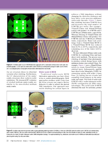
        Figure 4: A 200mm wafer-scale S-MCM fabrication approach with a combination of laser direct write and I-line   example, Figure 4 uses a 48mmX48mm
        photolithography: a) GDS layers to create wafer-scale S-MCM; b) A corresponding image of wafer-scale S-MCM;   reticle to create 96mmX96mm large
        and c-d) Enlarged optical micrographs of laser direct write based fan-out circuits.   stitched layers. Subsequently, applied
        the test structure shows no abnormal   Wafer-scale S-MCM              laser direct write lithography (LDW) for
        variation after stitching. Furthermore,   Tr a d it io n a l wa fe r- s c a le MC M   connecting reticles with wider (>1µm)
        the I-V characteristics of the snake/  fabrication approaches use laser direct   lines [3], adding fan-out circuits and
        combs structures show wafer-to-wafer   write or contact photolithography. Both   extending circuit features to the entire
        consistency. The measured RT resistance   approaches produce wider lines than   wafer real estate. This kind of wafer-scale
        of stitched niobium snake/combs are   the I-line process and require thicker   S-MCM with a wafer-interposer-wafer
        similar to the non-stitched niobium   dielectric in order to achieve the desired   (WIW) configuration [4] offers many
        snake/combs.                       50Ω  impedance.  Our  approach  uses   advantages. The wafer-scale S-MCM
                                           reticle stitching for critical layers to   eliminates the need  for substrates, printed


        Figure 5: A wafer-scale assembly process with a superconducting multichip module (S-MCM): a) I-line and LDW GDS layers for wafer-scale S-MCM; b) A corresponding
        wafer-scale S-MCM; c) Flip-chip wafer-scale bonded S-MCM with 20mm x 20mm superconducting test chip; and d) Schematic of wafer-to-wafer assembly options; (e)
        Schematic of a future 3D wafer-interposer-wafer (WIW) integration strategy. The superconducting chip, interposer, and wafer-scale S-MCMs are fabricated separately and
        joined together using flip-chip connection.

        22
        22   Chip Scale Review   January  •  February  •  2021   [ChipScaleReview.com]

