Page 31 - ChipScale_Jan-Feb_2021-digital
P. 31
to compensate for minor die shifts during
                                                                              RDL patterning will also contribute to
                                                                              overall panel yield.
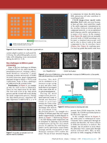
                                                                                CSAM inspection: mold voids
                                                                              detection. Mold voids can occur because
                                                                              of short gel time, short spiral flow length
                                                                              of the mold compound, contamination on
                                                                              the interface between silicon and mold
                                                                              compound material, or an un-optimized
                                                                              mold dispense profile and parameters,
                                                                              to name a few causes. In the example
                                                                              from Figure 8b, mold voids are normally
                                                                              detected with a CSAM metrology tool
                                                                              because a standard  microscope will
                                                                              not be able to detect voids at the mold
                                                                              compound to the Si interface layer
                                                                              (Figure 8a). Figure 8c confirms post-
                                                                              Cu stud top grind that mold voids were
        Figure 6: Die shift illustration from chip attach to post-mold cure.
        custom adaptive pattern to each panel [1].
        Utilizing this photolithography process
        helps with mitigating issues encountered
        during die shift (X, Y, Ɵ).
        Key challenges in 600mm panel
        processing
          Some of the key challenges in 600mm
        x 600mm PLP are die shift during the
        panelization process, warpage control,
        mold thickness variation, C-mode
        scanning acoustic microscopy (CSAM)   Figure 8: a) Example of CSAM defects: a) low magnification microscope; b) CSAM inspection; c) (four panels)
                                           Mold void after panel top grind post-CSAM.
        for defect detection, panel segmentation
        and panel design to satisfy a >99.5% yield   direction. This shift
        requirement. Some of these challenges   can be attributed to an
        are addressed in the sections below.  incorrect recipe set-up
          Panelization. In Figure 6, an example   or pick and place bond
        of why die shift occurs is illustrated.   heads that are not aligned
        There are two major areas for die shift.   to the center of the die, or
        The first will occur at the chip attach   to optical misalignment.
        process and the second will occur during   D u r i n g t h e  m ol d
        the mold compression process. During   compression  process,
        the chip attach process, singulated die   mold material tends to
        may experience a shift in the x, y or Ɵ   shrink and therefore
                                           te n d s   t o   g r a v i t a te
                                           towards the center of the
                                           panel. Consequently, this
                                           shrinkage also affects   Figure 9: CSAM mechanism for checking mold voids.
                                           die placement f rom                present from CSAM inspection. In this
                                           the previous process. An example of a   example, the CSAM is performed prior to
                                           600mm X 600mm panel that will require   the Dielectric 1 process.
                                           further improvements in mold dispense is   In the example shown in Figure 9,
                                           shown in Figure 7. Referencing Figure   the entire panel is submerged in water.
                                           7, die shift during mold compression can   Ultrasonic waves cannot pass through air
                                           be mitigated by applying a die position   pockets and therefore, the waves reflects
                                           compensation during the chip attach   at different interfaces or defects. For
                                           process. In addition, the mold dispense   example, any air pockets or areas where
                                           pattern can be optimized to ensure better   the ultrasonic wave cannot pass through
                                           coverage and the minimization of total   will be reflected 100%. This, in turn,
                                           thickness variation (TTV) within the
        Figure 7: Die position compensation and mold   panel. The use of laser directed imaging   provides us with a mapping of what the
        dispense need to be optimized.

                                                                                                             29
                                                          Chip Scale Review   January  •  February  •  2021   [ChipScaleReview.com]  29

