Page 37 - ChipScale_Jan-Feb_2021-digital
P. 37
device wafer during the thinning processes.
                                                                              The final Si has a TTV around 70nm—
                                                                              identical to the thickness variation of the
                                                                              epitaxially-grown Si layer. The wafers are
                                                                              then ready for nano-TSV processing.

                                                                              Nano-TSV formation
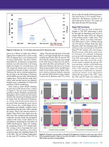
                                                                                The TSV process flow is shown in
                                                                              Figure 4. The TSV patterning is done
                                                                              by through-Si alignment and needs to
                                                                              ensure that the nano-TSVs are aligned
                                                                              to the bottom metal 1 (M1) layer. This
                                                                              requires <20nm of overlay tolerance.
                                                                              The TSVs have a 180 x 250nm oblong
                                                                              top CD and are 500nm deep (the final
                                                                              thickness after the thinning steps). TSV
                                                                              etching is also carried out on the SPTS
        Figure 3: Si thickness and TTV of the device wafer across the thinning process steps.  Rapier™ XE system, this time using a
                                                                              Bosch process with short cycle times
        grown on a 300mm Si wafer and a 500nm   ~20nm. The wet etch selectivity of Si to the   to minimize the sidewall scalloping
        capping layer of epitaxial Si is grown on top.   SiGe is not high enough that wet etching   and assist with subsequent depositions.
        This Si capping layer is the starting point   could be used for the entire Si removal. The   The TSV etch needs to stop on a thin
        for device fabrication. The SiGe content,   aim of the dry etching is to get close enough   dielectric layer that covers M1 as this
        being SiGe25%, is selected as a compromise   to the SiGe layer to allow the wet etch to   avoids metal re-sputtering during TSV
        between wet etch selectivity to Si (being   stop within the SiGe and not breach it. The   over-etching, which could otherwise
        higher for higher Ge concentration) and   SiGe layer thickness also has to be at least   lead to device reliability issues [4].
        film defectivity (being lower for lower Ge   50nm to prevent that. Finally, the SiGe layer   After  TSV  etching,  10nm  of  oxide
        concentration because of lattice mismatch).   itself is wet etched, using a highly SiGe-  is deposited conformally by plasma-
        Following the above substrate preparation,   to-Si selective chemical etchant, exposing   enhanced atomic layer deposition
        the next step is the fabrication of front-end-  the epitaxial 500nm-thick Si layer. Figure   (PEALD) throughout the TSV. Then
        of-line (FEOL) devices in the 500nm thick Si   3 shows the Si thickness and TTV of the   the TSV and M1 liners are etched in a
        capping layer. The top (device) wafer and a
        carrier wafer are then face-to-face dielectric
        bonded using a combination of 150nm SiO
        and 50nm of SiCN on both faces.
          After wafer-to-wafer (W2W) bonding,
        the next part of the process flow is shown
        in Figure 2. The top wafer is thinned by
        grinding to 50µm. Grinding is mechanically
        damaging to the Si surface and sub-surface,
        therefore the remaining Si thickness should
        be larger than the affected Si thickness,
        as cracks and disclocations must be
        prevented from reaching the active device
        areas, because they would impact device
        performance and reliability. A further 1µm is
        then polished from the Si by CMP to smooth
        the surface. Then a dry etch step removes a
        further 39µm of Si to leave 10µm above the
        SiGe layer. Dry etching benefits from being
        a high-rate step that avoids any mechanical
        contact to the wafer. It also allows for in
        situ thickness monitoring by near-infra-red
        (NIR) interferometry. After dry etching,
        the remaining Si has a TTV around 2µm.
        Dry etching is fast (~9µm/min) but is not
        selective to SiGe. Therefore, a wet etch is
        needed to remove the remaining 10µm of Si
        to the SiGe. The wet etching compensates   Figure 4: TSV patterning process flow: a) Through Si-TSV alignment to bottom M1 and dry etch, stop on STI; b)
        for the 2µm TTV leaving a SiGe TTV at   PEALD oxide liner deposition (10nm) and liner etch (TSV) bottom; c) TSV metallization (Cu electroplating) and Cu
                                           CMP; d) Back-side metal processing (BSM1).

                                                                                                             35
                                                          Chip Scale Review   January  •  February  •  2021   [ChipScaleReview.com]  35

