Page 43 - ChipScale_Jan-Feb_2021-digital
P. 43
Figure 4: CF inspection results shown in a composite
                                                                              panel map.
                                                                              metal layer permits extremely sensitive
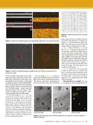
        Figure 2: a) (left) CF and b) (right) BF images of 2µm horizontal RDL captured with a 10X objective (0.7µm/pixel)  inspection with detection of single-pixel
                                                                              defects. A short between the upper two
                                                                              RDL lines that was not seen in the BF
                                                                              image is clearly visible in the CF image.
                                                                                Figure 3 shows 10X CF (Figure 3a) and
                                                                              BF (Figure 3b) images of the same area
                                                                              of vertically oriented 3.5µm RDL lines on
                                                                              a panel. The grainy metal surface and the
                                                                              noisy background in the BF image prevent
                                                                              clear visibility of the edges and continuity
                                                                              of the RDL lines. Unlike the BF image, the
                                                                              boundaries and the continuity of the RDLs
                                                                              can be clearly seen in the CF image. A
                                                                              short can be seen between the RDL lines
                                                                              in the CF image. The same short is not
                                                                              visible in the BF image.
                                                                                Figure 4 shows the CF inspection
                                                                              results of RDL lines on a panel. The
        Figure 3: a) (left) CF and b) (right) BF images of vertically oriented 3.5µm RDL lines captured with the 10X
        objective (0.7µm/pixel)                                               dots on the panel map represent defect
                                                                              locations. More defects were found on
        shows a bright field image of the same   The CF image (Figure 2a) shows a   the right side of the panel and there
        area. In the areas circled in red, three 2µm   clear contrast difference between the metal   appears to be a repeating pattern within
        RDL lines separated by 2µm spaces run   RDL lines and the underlying polymer.   each die/package.
        horizontally across the image. A wider band   The absence of texture and graininess   Through-silicon via sample. The next
        of organic polymer runs beneath the RDL   in the metal RDL lines and underlying   is a large panel with through-silicon vias
        lines, isolating them from an underlying
        layer of metal. Contrast is reversed between
        the CF and BF images – metal is dark and
        polymer bright in the CF image, while
        metal is bright, and polymer is semi-
        transparent and darker in the BF image.
          In the BF image (Figure 2b), the
        underlying metal surface showing
        through the polymer film looks very
        much like the RDL lines, making
        it difficult to distinguish the upper
        layer metal features from the material
        below. The graininess of the metal also
        obscures real defects and interferes
        with the automatic detection algorithm.
        Inspection  of  this  sample  with  BF
        illumination resulted in high nuisance
        defect counts without finding real
        process issues on the wafer.       Figure 5: TSV images captured with a) (left) BF, b) (middle) DF, and c) (right) CF  illumination using the 10X
                                           objective (0.7µm/pixel)

                                                                                                             41
                                                          Chip Scale Review   January  •  February  •  2021   [ChipScaleReview.com]  41

