Page 44 - ChipScale_Jan-Feb_2021-digital
P. 44
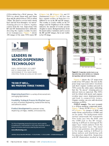
(TSVs) drilled for a 3D-IC process. The   (Figure 5a), DF (Figure 5b), and CF
        TSVs are about 30µm wide and 20µm   illumination (Figure 5c). All four vias
        deep and the pitch between TSVs is about   have organic residue in them but it is
        120µm. The panel is covered with a metal   difficult to see in the BF and DF images.
        layer and has been through a “de-smear”   The residue is clearly visible in the CF
        cleaning process to remove organic   images and the brightness of the residue
        residue from the vias. Inspections with   indicates the amount of residue present
        BF and DF illumination have difficulty   (brighter is more). Background noise from
        detecting the organic residue because   the metal surface variations can be seen in
        of its transparency. Figure 5 shows   the BF and DF images, but is not visible
        10X images of the same TSVs under BF   in the CF image.


             LEADERS IN
             MICRO DISPENSING

             TECHNOLOGY


             SMALL REPEATABLE VOLUMES
             ARE A CHALLENGE, BUT NOT
             IMPOSSIBLE IF YOU HAVE BEEN                                      Figure 6: CF inspection results shown as a a)
             CREATING THEM AS LONG AS WE HAVE.                                (top) defect map, and b) (bottom) as a histogram
                                                                              distinguishing lighter and heavier deposits.

                                                                                Figure 6 shows the CF inspection
             TO DO IT WELL,                                                   result of the TSV panel. The dots on the
                                                                              panel map represent defect locations
             WE PROVIDE THREE THINGS:                                         and show organic residues present in
                                                                              TSVs across the entire panel, indicating
                                                                              that the “de-smear” cleaning process
                                                                              did not work as expected. The TSVs
             Dispensing Expertise in a variety of microelectronic             will be filled with metal and organic
             packaging applications.                                          residue may cause deplanarization
                                                                              and lead to con nect ivit y issues.
             Feasibility Testing & Process Verification based                 Organic residue can also add electrical
             on years of product engineering, material flow testing           resistance in TSVs.
             and software control.                                              FOPLP sample. The next example
                                                                              is a 450mm molding compound panel.
             Product Development for patented valves,                         Figure 7 shows 4X BF (Figure 7a) and
             dispensing cartridges, needles, and accessories.                 CF (Figure 7b) images of RDL and
                                                                              under bump metallization (UBM) pad
                                                                              on the panel. The background metal
                                                                              surface  underneath  the  transparent
                                                                              f ilm  looks  just  like  the  RDL  and
                                                                              t h e U BM p a d i n t h e BF i m a ge ,
                                                                              making it difficult to distinguish the
             Our Micro Dispensing product line is proven and trusted by
             manufacturers in semiconductor, electronics assembly, medical    upper layer metal patterns from the
             device and electro-mechanical assembly the world over.           underlying  metal  layer.  The metal
                                                                              texture and graininess also add noise
             www.dltechnology.com.
                                                                              to the image, making it difficult to
                                                                              detect defects and interfering with
             216 River Street, Haverhill, MA 01832  •  P: 978.374.6451  •  F: 978.372.4889  •  info@dltechnology.com  the detection algorithm. Inspection
                                                                              with BF illumination resulted in high

        42   Chip Scale Review   January  •  February  •  2021   [ChipScaleReview.com]
        42

