Page 51 - ChipScale_Jan-Feb_2021-digital
P. 51
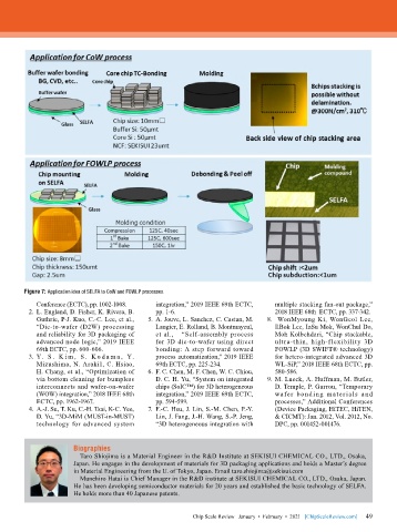
Figure 7: Application idea of SELFA to CoW and FOWLP processes.
            Conference (ECTC), pp. 1002-1008.  integration,” 2019 IEEE 69th ECTC,   multiple stacking fan-out package,”
          2.  L. England, D. Fisher, K. Rivera, B.   pp. 1-6.                     2018 IEEE 68th  ECTC, pp. 337-342.
            Guthrie, P-J. Kuo, C.-C. Lee, et al.,   5.  A. Jouve, L. Sanchez, C. Castan, M.   8.   WonMyoung Ki, WonGeol Lee,
            “Die-to-wafer (D2W) processing     Laugier, E. Rolland, B. Montmayeul,   IlBok Lee, InSu Mok, WonChul Do,
            and reliability for 3D packaging of   et al.,   “Self-assembly process   Moh Kolbehdari, “Chip stackable,
            advanced node logic,” 2019 IEEE    for 3D die-to-wafer using direct   ultra-thin, high-f lexibility 3D
            69th ECTC, pp. 600-606.            bonding: A step forward toward     FOWLP (3D SWIFT® technology)
          3.  Y. S . K i m , S . K o d a m a , Y.   process automatization,” 2019 IEEE   for hetero-integrated advanced 3D
            Mizushima, N. Araki1, C. Hsiao,    69th ECTC, pp. 225-234.            WL-SiP,” 2018 IEEE 68th ECTC, pp.
            H. Chang, et al., “Optimization of   6.  F. C. Chen, M. F. Chen, W. C. Chiou,   580-586.
            via bottom cleaning for bumpless   D. C. H. Yu, “System on integrated   9.  M. Lueck, A. Huffman, M. Butler,
            interconnects and wafer-on-wafer   chips (SoIC™) for 3D heterogeneous   D. Temple, P. Garrou, “Temporary
            (WOW) integration,” 2018 IEEE 68th   integration,” 2019 IEEE 69th ECTC,   wafer bondi ng mater ials and
            ECTC, pp. 1962-1967.               pp. 594-599.                       processes,” Additional Conferences
          4.  A.-J. Su, T. Ku, C.-H. Tsai, K-C. Yee,   7.  F.-C. Hsu, J. Lin, S.-M. Chen, P.-Y.   (Device Packaging, HiTEC, HiTEN,
            D. Yu, “3D-MiM (MUST-in-MUST)      Lin, J. Fang, J.-H. Wang, S.-P. Jeng,   & CICMT): Jan. 2012, Vol. 2012, No.
            technology for advanced system     “3D heterogeneous integration with   DPC, pp. 001452-001476.


                       Biographies
                         Taro Shiojima is a Material Engineer in the R&D Institute at SEKISUI CHEMICAL CO., LTD., Osaka,
                       Japan. He engages in the development of materials for 3D packaging applications and holds a Master’s degree
                       in Material Engineering from the U. of Tokyo, Japan. Email taro.shiojima@sekisui.com
                         Munehiro Hatai is Chief Manager in the R&D institute at SEKISUI CHEMICAL CO., LTD., Osaka, Japan.
                       He has been developing semiconductor materials for 20 years and established the basic technology of SELFA.
                       He holds more than 40 Japanese patents.


                                                                                                             49
                                                          Chip Scale Review   January  •  February  •  2021   [ChipScaleReview.com]  49

