Page 56 - ChipScale_Jan-Feb_2021-digital
P. 56
TECHNOLOGY TRENDS


                           Adhesive bonding for flexible microLED


                           display assembly


                           By Goutham Ezhilarasu, Subramanian Iyer  [UCLA]  Ajit Paranjpe [Veeco Instruments, Inc.]
                           Jay Lee  [DISCO Corporation]  Frank Wei  [DISCO Hi-Tec America, Inc.]
        I     n recent years, there has been   thickness), sequential pick and place for   action of a voltage-driven stamp to attract


              growing interest in fabricating high-
                                           assembly is impractical. Therefore, a mass
                                                                              and pickup microLEDs for transfer. This
              resolution information displays using
                                           a large block of devices from the growth
              micro-scale inorganic light emitting   transfer process is generally used wherein   approach is very sensitive to substrate
                                                                              planarity and surface contamination, and
        diodes (i.e., microLEDs) as an alternative   substrate are transferred and assembled onto   involves a relatively complex process with
        to organic LED (OLED) or liquid crystal   the target in a massively parallel fashion [2]   specialized equipment such as an active
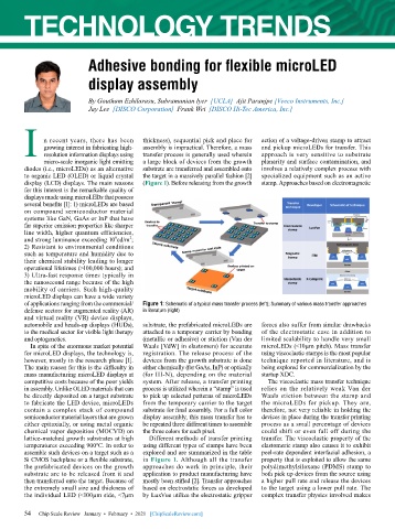
        display (LCD) displays. The main reasons   (Figure 1). Before releasing from the growth   stamp. Approaches based on electromagnetic
        for this interest is the remarkable quality of
        displays made using microLEDs that possess
        several benefits [1]: 1) microLEDs are based
        on compound semiconductor material
        systems like GaN, GaAs or InP that have
        far superior emission properties like sharper
        line width, higher quantum efficiencies,
        and strong luminance exceeding 10 cd/m ;
                                   6
                                       2
        2) Resistant to environmental conditions
        such as temperature and humidity due to
        their chemical stability leading to longer
        operational lifetimes (>100,000 hours); and
        3) Ultra-fast response times typically in
        the nanosecond range because of the high
        mobility of carriers. Such high-quality
        microLED displays can have a wide variety
        of applications ranging from the commercial/  Figure 1: Schematic of a typical mass transfer process (left); Summary of various mass transfer approaches
        defense sectors for augmented reality (AR)   in literature (right)
        and virtual reality (VR) device displays,
        automobile and heads-up displays (HUDs),   substrate, the prefabricated microLEDs are   forces also suffer from similar drawbacks
        to the medical sector for visible light therapy   attached to a temporary carrier by bonding   of the electrostatic case in addition to
        and optogenetics.                  (metallic or adhesive) or stiction (Van der   limited scalability to handle very small
          In spite of the enormous market potential   Waals [VdW] in elastomers) for accurate   microLEDs (<10µm pitch). Mass transfer
        for microLED displays, the technology is,   registration. The release process of the   using viscoelastic stamps is the most popular
        however, mostly in the research phase [1].   devices from the growth substrate is done   technique reported in literature, and is
        The main reason for this is the difficulty in   either chemically (for GaAs, InP) or optically   being explored for commercialization by the
        mass manufacturing microLED displays at   (for III-N), depending on the material   startup XDC.
        competitive costs because of the poor yields   system. After release, a transfer printing   The viscoelastic mass transfer technique
        in assembly. Unlike OLED materials that can   process is utilized wherein a “stamp” is used   relies on the relatively weak Van der
        be directly deposited on a target substrate   to pick up selected patterns of microLEDs   Waals stiction between the stamp and
        to fabricate the LED device, microLEDs   from the temporary carrier to the target   the microLEDs for pickup. They are,
        contain a complex stack of compound   substrate for final assembly. For a full color   therefore, not very reliable in holding the
        semiconductor material layers that are grown   display assembly, this mass transfer has to   devices in place during the transfer printing
        either epitaxially, or using metal organic   be repeated three different times to assemble   process as a small percentage of devices
        chemical vapor deposition (MOCVD) on   the three colors for each pixel.  could shift or even fall off during the
        lattice-matched growth substrates at high   Different methods of transfer printing   transfer. The viscoelastic property of the
        temperatures exceeding 900ºC. In order to   using different types of stamps have been   elastomeric stamp also causes it to exhibit
        assemble such devices on a target such as a   explored and are summarized in the table   peel-rate dependent interfacial adhesion, a
        Si CMOS backplane or a flexible substrate,   in Figure 1. Although all the transfer   property that is exploited to allow the same
        the prefabricated devices on the growth   approaches do work in principle, their   polydimethylsiloxane (PDMS) stamp to
        substrate are to be released from it and   application to product manufacturing have   both pick up devices from the source using
        then transferred onto the target. Because of   mostly been stifled [2]. Transfer approaches   a higher pull rate and release the devices
        the extremely small size and thickness of   based on electrostatic forces as developed   to the target using a lower pull rate. The
        the individual LED (<100µm side, <7µm   by LuxVue utilize the electrostatic gripper   complex transfer physics involved makes

        54
        54   Chip Scale Review   January  •  February  •  2021   [ChipScaleReview.com]

