Page 54 - ChipScale_Jan-Feb_2021-digital
P. 54
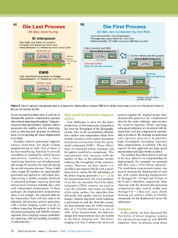
Figure 3: Direct imaging for heterogeneous devices: a) Approaches utilizing silicon interposer/EMIB where all dies need a bump; and b) a die-first approach where all
        dies are connected by fine RDL.
        the pre-measured position data of each die to   High-speed compensation exposure   position against the original design data,
        dynamically generate compensated exposure   system                    dynamically generates the compensated
        data without impacting throughput. Using pre-  One challenge to date for the mass   data for the entire substrate, and executes
        measured data and dynamic exposure pattern   production of heterogeneous integration   the scanned exposure. While exposing,
        generation also enables selective patterning,   has been the throughput of the lithography   subsequent substrates are measured with the
        such as selecting pad openings in arbitrary   system. Dies on the reconstituted substrate   stand-alone tool and compensated exposure
        areas, or not exposing die whose displacement   have random and independent offsets from   data is produced. By utilizing measurement
        is too large.                      mounter accuracy errors and/or movement   and exposure processes in parallel,
          Dynamic pattern generation supports   (expansion/contraction) from the epoxy   high throughput, including exposure
        unique  functions  for  high-volume   mold compound (EMC). These offsets   data compensation, is realized. The key
        manufacturing as well. One of these is   must be measured before exposure and   aspects for this approach are high-speed
        an auto-numbering function to provide   the pattern modified to compensate. This   measurement and high overlay accuracy.
        traceability as required for critical devices   measurement time increases with the   The method described above is proven
        (automotive, healthcare, etc.). Auto-  number of dies on the substrate, further   to be very effective at compensating for
        numbering functions can simultaneously   reducing the throughput of the exposure   displacement. For example, we mounted
        add unique ID numbers for each die during   system. However, we have shown it is   600 dies onto a 515x510mm substrate.
        the normal exposure process. Using simple   possible to pre-measure the die with a stand-  The stand-alone measurement system was
        rules, unique ID numbers are automatically   alone tool to realize the full advantages of   used to measure the displacement of each
        generated and applied to individual dies.   the direct imaging approach (Figure 2). In   die, with results showing displacements
        Auto-wiring is another example, beneficial   the measurement tool, the exact positions   of |Average|+3σ = 81.5µm and 162.0µm in
        to advanced packages requiring electrical   of all dies are recorded. Twin time delay   the X and Y directions, respectively. After
        interconnects between multiple dies, each   integration (TDI) cameras are used to   exposing with the dynamically-generated
        with independent displacement. In these   scan the substrate and create an image   compensation data, overlay results were
        packages, die displacement compensation   of the entire surface. Our algorithm then   |Average|+3σ = 1.9µm and 1.4µm, clearly
        alone is not enough—the exposure data for   efficiently and rapidly extracts localized   showing our system’s ability to flexibly
        the interconnect lines will also need to be   images, wherein alignment mark matching   compensate for die displacement across the
        adjusted, and dynamic pattern generation   is performed on each die. With this system,   entire panel.
        with a direct imaging system can do so   the measurement time for 5,000 mounted
        without impacting throughput. In both the   dies on a 515x510 substrate is as low as   Summary
        advanced packaging and MEMS industry   120s. After measurement, the substrate   In this article, we have discussed the
        segments, direct imaging’s unique capabilities   design and measurement data are loaded   flexibility of direct imaging systems
        are improving yield and enabling traceability   to the direct imaging tool. The direct   for advanced packaging and MEMS
        of critical devices.               imaging tool then evaluates the measured   industries. Now, we propose using direct


        52
        52   Chip Scale Review   January  •  February  •  2021   [ChipScaleReview.com]

