Page 43 - ChipScale_May-June_2020-digital
P. 43
Figure 2: Cross-section workflow comparisons.
        Cu-pillar microbumps in a 3D       electrons. The laser quality allows imaging   sectioned microbump void superimposed
        package                            of some structures right after laser polishing.   upon the virtual plan-view XRM slice that
                                              +
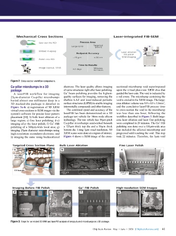
          A laserFIB workflow for imaging   Ga  beam polishing provides the highest-  guided the laser cuts. The void is indicated by
        25µm-diameter Cu-pillar microbumps   quality surfaces for imaging, removing the   a red arrow. The microbump containing the
        buried almost one millimeter deep in a   shallow LAZ and laser-induced periodic   void is circled in the XRM image. The large-
                                                                                                              3
        3D stacked-die package is detailed in   surface structures (LIPSS) to enable imaging   area ablation volume was 0.9 x 0.9 x 1.0mm ,
        Figure 3a-h: a) registration of 3D XRM   intermetallic compounds and other features.  and the cumulative laserFIB process time
        virtual cross-sections to SEM images via the   The combined speed and accuracy of the   to cross-section the void in the microbump
        system’s software for precise laser pattern   laserFIB has been demonstrated on a 3D   was less than one hour, following the
        placement [10]; b) bulk laser ablation of a   package test vehicle for 14nm node silicon   workflow described in Figure 3. Both large-
        large region; c) fine laser polishing; d-e)   technology. The test vehicle has 50µm pitch   area laser ablation and laser fine polishing
                                                                                                           +
                                    +
        imaging after the laser polish; f) Ga  FIB   Cu-pillar microbumps sandwiched beneath   were completed in 29 minutes. The Ga  FIB
        polishing of a 300µm-wide local area; g)   a 725µm thick top die and a 50µm thick   polishing was done over a 110µm-wide area
        imaging 25µm diameter microbumps using   bottom die. Using 1µm voxel resolution, 3D   that included the affected microbump and
        high-resolution secondary-electrons; and   XRM scans were done at a region of interest.   progressed until reaching the void. This step
        h) imaging the same using backscattered   Figure 4 shows a SEM image of the cross-  took 22 minutes. Therefore, the 5µm void


        Figure 3: Steps for correlated 3D XRM and laserFIB analysis of deeply buried microbumps in a 3D package.

                                                                                                             41
                                                               Chip Scale Review   May  •  June  •  2020   [ChipScaleReview.com]  41

