Page 44 - ChipScale_May-June_2020-digital
P. 44
3.  L. Mirkarimi, “The proliferation of
                                                                                  hybrid bonding for 3D integrated
                                                                                  circuits,” presented at the 3D &
                                                                                  Systems Summit, Dresden, 2020.
                                                                                4.  J. Ryckaert, E. Beyne, “A 3D
                                                                                  technology toolbox in support of
                                                                                  system-technology co-optimization,
                                                                                  imec Magazine, 2019.
                                                                                5. C. Hartfield, C. Schmidt, A. Gu,
                                                                                  S. T. Kelly, “From PCB to BEOL:
                                                                                  3D X-ray microscopy for advanced
                                                                                  semiconductor packaging,” Inter.
                                                                                  Physics of Failure Analysis, Marina
                                                                                  Bay Sands Conv. Center, Singapore,
                                                                                  2018.
                                                                                6. ZEISS Xradia 610 and 620 Versa
                                                                                  Product Information, version 1.1.
                                                                                  (2019).
                                                                                7.  P. S. Pichumani, F. Khatkhatay,
                                                                                  “Mechanical milling and polishing
                                                                                  of cross sections using a micro
                                                                                  CNC machine for failure analysis,”
                                                                                  Electronic Device Failure Analysis
                                                                                  (EDFA), 14-19 (2020).
                                                                                8. K. Sugioka, Y. Cheng, “Ultrafast
                                                                                  lasers—reliable tools for advanced
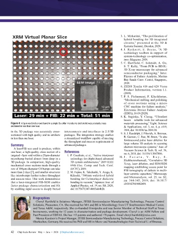
        Figure 4: A 5µm void (red arrow) found in a single Cu-pillar microbump (red circle) was precisely cross   materials processing,” Light: Science
        sectioned in less than one hour.                                          & Applications, vol. 3, no. 4, p. e149,
        in the 3D package was accurately cross-  interconnects and interfaces in 2.5/3D   2014, doi: 10.1038/lsa.2014.30.
        sectioned with high quality and no artifacts   packages. The integration strategy enables   9.  S. J. Randolph, J. Filevich, A. Botman,
        in less than one hour.             a streamlined workflow capable of meeting   R. Gannon, C. Rue, M. Straw, “In situ
                                           the throughput and success requirements of   femtosecond pulse laser ablation for
        Summary                            advanced packages.                     large volume 3D analysis in scanning
                                                                                  electron microscope systems,” Jour. of
          A laserFIB was used to produce, within                                  Vacuum Science & Tech. B, vol. 36,
        one hour, a high-quality cross section of a   References                  no. 6, 2018, doi: 10.1116/1.5047806.
        targeted ~5µm void within a 25µm-diameter   1.  P. Coudrain, et al., “Active interposer   10.  J . F a v a t a , V . R a y , S .
        microbump buried almost 1mm deep in a   technology for chiplet-based advanced   Shahbazmohamadi, “Correlative 3D
        3D package. In comparison, high-quality   3D system architectures,” 2019 IEEE   X-ray, laser ablation, and SEM/EDS
        mechanical cross sections made through a   69th Elec. Comp. and Tech. Conf.   mapping establishing access point for
        row of 100µm-diameter C4 bumps can take   (ECTC), 2019.                   FIB tomography of defects in multi-
        more than 2 days [7], and smaller structures   2. M. Fujino, K. Takahashi, Y. Araga, K.   layer ceramic capacitors,” Microscopy
        like microbumps further reduce throughput   Kikuchi, “300mm wafer-level hybrid   and Microanalysis, vol. 25, no. S2,
        and success rates. This work demonstrates   bonding for Cu/interlayer dielectric   pp. 344-345, 2019, doi: 10.1017/
        that a laser-integrated FIB-SEM enables   bonding in vacuum,” Japanese Jour. of   s1431927619002459.
        faster package characterization and FA   Applied Physics, vol. 59, no. SB, 2020,
        by enabling rapid access to deeply buried   doi: 10.7567/1347-4065/ab4b2b.


                       Biographies
                         Cheryl Hartfield is Solutions Manager, ZEISS Semiconductor Manufacturing Technology, Process Control
                       Solutions, Pleasanton, CA. She received her MA and BS in Microbiology from UT Southwestern Medical Center,
                       and Texas A&M, respectively. She co-founded Omniprobe and was Senior Member of Technical Staff at Texas
                       Instruments, working for 12 years in characterization and package development. Cheryl is an ASM Fellow and
                       Past President of EDFAS. She has >13 patents and authored >70 papers. Email cheryl.hartfield@zeiss.com
                         Marcus Kaestner is Project Manager, ZEISS Semiconductor Manufacturing Technology, Process Control Solutions,
                       Oberkochen, Germany. He received his PhD and MS in Micro- and Nanotechnologies from Technical U. of Ilmenau.


        42   Chip Scale Review   May  •  June  •  2020   [ChipScaleReview.com]
        42

