Page 46 - ChipScale_May-June_2020-digital
P. 46
The next step: reducing the spacing
                                                                              between p and n
                                                                                As the journey to smaller track heights
                                                                              continues, a further reduction of cell
                                                                              height will require a much tighter spacing
                                                                              between nFET and pFET devices within
                                                                              the cell. However, for both FinFET and
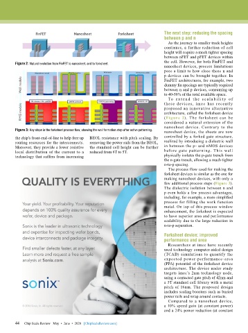
        Figure 2: Natural evolution from FinFET to nanosheet, and to forksheet.
                                                                              nanosheet devices, process limitations
                                                                              pose a limit to how close these n and
                                                                              p devices can be brought together. In
                                                                              FinFET architectures, for example, two
                                                                              dummy fin spacings are typically required
                                                                              between n and p devices, consuming up
                                                                              to 40-50% of the total available space.
                                                                                To e x t e n d t h e s c a l a b i l i t y o f
                                                                              these devices, imec has recently
                                                                              proposed an innovative alternative
                                                                              architecture, called the forksheet device
                                                                              (Figure 2). The forksheet can be
                                                                              considered a natural extension of the
                                                                              nanosheet device. Contrary to the
        Figure 3: Key steps in the forksheet process flow, showing the wall formation step after active patterning.  nanosheet device, the sheets are now
        the chip’s front-end-of-line to help free up   BEOL resistance with pitch scaling. By   controlled by a forked gate structure,
        routing resources for the interconnects.   removing the power rails from the BEOL,   realized by introducing a dielectric wall
        Moreover, they provide a lower resistive   the standard cell height can be further   in between the p- and nMOS devices
        local distribution of the current to a   reduced from 6T to 5T.       before gate patterning. This wall
        technology that suffers from increasing                               physically isolates the p-gate trench from
                                                                              the n-gate trench, allowing a much tighter
                                                                              n-to-p spacing.
                                                                                The process flow used for making the
                                                                              forksheet devices is similar as the one for
                                                                              making nanosheet devices, with only a
                                                                              few additional process steps (Figure 3).
                                                                              The dielectric isolation between n and
                                                                              p even holds a few process advantages,
                                                                              including, for example, a more simplified
                                                                              process for filling the work function
                                                                              metal. On top of this process window
                                                                              enhancement, the forksheet is expected
                                                                              to have superior area and performance
                                                                              scalability due to the large reduction in
                                                                              n-to-p separation.

                                                                              Forksheet device: improved
                                                                              performance and area
                                                                                Researchers at imec have recently
                                                                              used technology computer-aided design
                                                                              (TCAD) simulations to quantify the
                                                                              expected power-performance-area
                                                                              (PPA) potential of the forksheet device
                                                                              architecture. The device under study
                                                                              targets imec’s 2nm technology node,
                                                                              using a contacted gate pitch of 42nm and
                                                                              a 5T standard cell library with a metal
                                                                              pitch of 16nm. The proposed design
                                                                              includes scaling boosters such as buried
                                                                              power rails and wrap around contacts.
                                                                                Compared to a nanosheet device,
                                                                              a 10% speed gain (at constant power)
                                                                              and a 24% power reduction (at constant


        44
        44   Chip Scale Review   May  •  June  •  2020   [ChipScaleReview.com]

