Page 47 - ChipScale_May-June_2020-digital
P. 47
speed) was calculated. This performance
        boost can  be partly  explained  by  a
        reduced (parasitic) Miller capacitance,
        resulting from a smaller gate-drain
        overlap. The available space can also be
        used to increase the sheet width, and as
        such, enhance the drive current. Finally,
        the n-to-p separation reduction can be
        exploited for shrinking the track height
        from 5T to 4.3T – resulting in a 20%
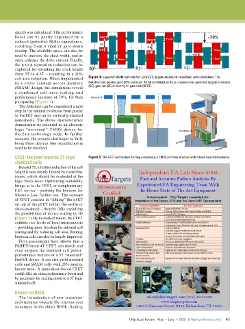
        cell area reduction. When implemented   Figure 4: Layout of SRAM half cells for: a) FinFET; b) gate-all-around nanosheet; and c) forksheet. The
        in a static random access memory   forksheet can provide up to 30% scaling of the bit cell height as the p-n space is not governed by gate extension
        (SRAM) design, the simulations reveal   (GE), gate cut (GE) or dummy fin gate tuck (DFGT).
        a combined cell area scaling and
        performance increase of 30%, for 8nm
        p-n spacing (Figure 4).
          The forksheet can be considered a next
        step in the natural evolution from planar
        to FinFET and on to vertically-stacked
        nanosheets. The above characteristics
        demonstrate its potential as an ultimate
        logic “universal” CMOS device for
        the 2nm technology node. In further
        research, the process challenges to fully
        bring these devices into manufacturing
        need to be resolved.

        CFET: the road towards 3T logic    Figure 5: The CFET architecture forming a stacked p-n CMOS primitive structure with 2-level local interconnects.
        standard cells
          Beyond 5T, a further reduction of the cell
        height is now mainly limited by routability
        issues, which should be evaluated at the
        logic block level. Optimizing routability
        brings us to the CFET, or complementary
        FET device – pushing the horizon for
        Moore’s Law further out. The concept
        of CFET consists in “folding” the nFET
        on top of the pFET (either fin-on-fin or
        sheet-on-sheet) – thereby fully exploiting
        the possibilities of device scaling in 3D
        (Figure 5). By its stacked nature, the CFET
        exhibits two levels of local interconnects
        – providing more freedom for internal cell
        routing and for reducing cell area. Routing
        between cells can also be largely improved.
          First assessments have shown that a
        FinFET-based 4T CFET can match and
        even surpass the standard cell power-
        performance metrics of a 5T “standard”
        FinFET device. It can also yield standard
        cells and SRAM cells with 25% smaller
        layout area. A nanosheet-based CFET
        could offer an extra performance boost and
        be necessary for scaling down to a 3T logic
        standard cell.

        Impact on BEOL
          The introduction of new transistor
        architectures impacts the interconnect
        structures in the chip’s BEOL. Scaling


                                                                                                             45
                                                               Chip Scale Review   May  •  June  •  2020   [ChipScaleReview.com]  45

